SiC, the new silicon?
Driven by the energy transition and electromobility, there is currently a rapidly growing demand for electronic components for the particularly low-loss conversion of electrical energy. A prominent topic in semiconductor technology is therefore the so-called WBG or wide-bandgap semiconductors, such as silicon carbide, gallium nitride or aluminum nitride. They can withstand high voltages at very low forward losses and thus offer the best prerequisites for building highly efficient power electronic systems. Among the WBG semiconductor materials, silicon carbide (SiC) in particular has become established, and a wide range of commercial products is already available. In areas of application where the highest power densities and highest power conversion efficiencies are required, SiC devices with their superior electrical properties are already displacing conventional silicon power electronics. This is the case, for example, in the wiring systems and drive electronics of electric vehicles or in the connection of renewable energy sources to the public power grid.
Class instead of mass
The special physical properties of the WBG semiconductor silicon carbide open up further interesting application possibilities, such as in optoelectronics and sensor technology or for future solid-state quantum electronics. For example, the Berlin-based high-tech company sglux relied on SiC sensor components at an early stage and successfully established itself on the market with SiC photodiodes for measuring ultraviolet radiation (UV). These photodiodes are used wherever safety has top priority. This is the case, for example, in medical technology for monitoring dialysis, in food processing for controlling sterilization processes, or in industry for controlling combustion processes. The core components for the UV diodes, SiC chips with SiC heterostructures, are processed at Fraunhofer IISB in Erlangen according to sglux specifications on the institute’s own SiC CMOS line.
SiC conquers space
Artistic representation of the landing of the Mars rover Perseverance on Mars in the Jezero crater on February 18, 2021. The main goals of NASA’s MARS 2020 mission are to search for signs of past life and to collect rock and soil samples for later return to Earth.
One of the most challenging operating environments for electronic components is certainly space. Here, all components must function absolutely reliably under extreme conditions, and even the smallest errors or failures can endanger the entire mission. Against this background, it is a great success for sglux GmbH from Berlin and also for Fraunhofer IISB that even NASA now belongs to the customer base of the SiC pioneers. During NASA’s current MARS 2020 mission, a SiC UV photodiode from sglux also landed on the red planet with the Mars rover Perseverance on February 18, 2021, and has been functioning reliably ever since.
The extraordinary environment provides the perfect opportunity to demonstrate the reliability of sglux’s products and the quality of the SiC sensors manufactured in small series at IISB. “Perseverance” – which means perseverance, endurance or perseverance in German – is the most advanced and elaborate rover NASA has ever sent to Mars. The roughly two-and-a-half-billion-dollar exploration vehicle searches the Martian surface for traces of past microbial life and characterizes the planet’s geology and climate, in part to prepare for a future manned mission to Mars.
Life on Mars
Cutting-Edge Technology on the Mars Rover: Perseverance has seven sophisticated scientific instruments for detailed examination of its environment. The exploration vehicle has a robotic arm with the SHERLOC deep-UV Raman spectrometer mounted on the end.
Perseverance has a suite of advanced science instruments, among which a deep-UV Raman spectrometer mounted on the rover’s robotic arm plays a special role. Dubbed SHERLOC (Scanning Habitable Environments with Raman & Luminescence for Organics & Chemicals), the high-tech instrument is the first ever UV Raman spectrometer on Mars. There, it enables the non-contact, spatially resolved and highly sensitive detection and characterization of organic substances and minerals on the surface and in the near subsurface. On Earth, by contrast, Raman spectroscopy, named after physicist C. V. Raman, is used, for example, to study the material properties of semiconductor crystals.
Aided by a special camera called WATSON (Wide Angle Topographic Sensor for Operations and eNgineering) and a UV LASER, SHERLOC detects organic matter and minerals and creates topographic maps of them. Research teams on Earth then evaluate the measurement results and mineralogical maps to see if there is evidence of past water influence and evidence of past life on Mars. Based on this, a decision will be made as to which rock samples Perseverance should take and leave sealed in metal tubes on the Martian surface for a future return to Earth (resample mission).
Absolute endurance test
Detailed image of the SHERLOC deep-UV Raman spectrometer on the Mars rover Perseverance. The UV spectrometer is equipped, among other things, with a SiC UV photodiode processed at Fraunhofer IISB in Erlangen, Germany, by the Berlin-based company sglux. The UV sensor with TO5 housing is mounted to the left of the camera lens and measures the radiation power of the Raman spectrometer in the deep UV range.
For its measurements, the UV Raman spectrometer uses a deep UV laser with a wavelength of 248.6 nm focused on a spot less than 100 µm in diameter. A SiC UV broadband photodiode of type SG01XL-5 from sglux is installed near the laser aperture. This detects the UV radiated power emitted by SHERLOC during spectral mapping, allowing the laser’s performance to be monitored as it scans the surface.
Prior to its deployment, sglux adapted the photodiode’s manufacturing process to the mission and performed extensive selection, testing and characterization procedures. Subsequently, NASA subjected the candidates thus selected to further tests and trials, for example on vibration resistance, behavior under strong acceleration, high-temperature resistance and alternating resistance.
Unique material properties
Highly reliable, space-qualified and daylight-insensitive SG01XL-5 broadband SiC UV photodiode from sglux in a proven TO5 package. The aging-resistant, low-noise and fast-response SiC UV sensor operates stably over a wide temperature range. The 7.6 x 7.6 mm² silicon carbide chip, processed at Fraunhofer IISB, can be seen in the center of the package.
Because of its unique properties, silicon carbide is currently the best semiconductor material for UV detectors that are insensitive to daylight and is ideal for use in difficult environments. The SiC-based photodiodes are almost completely blind to light in the visible waveband and have an impressive response speed. The small dark current in the femtoampere range ensures low noise, so that even very low UV radiation intensities can be reliably measured.
The SiC detectors tolerate comparatively high operating temperatures and operate stably in a temperature range of minus 55 to plus 170 °C. Here, the temperature coefficient of the signal reaches values of less than 0.1 % per Kelvin and temperature-related changes in measurement sensitivity can be well compensated. In addition, SiC has extreme radiation hardness, which allows the devices to retain their excellent electrical properties even under long and strong irradiation.
Business and Science
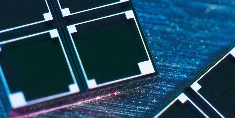
Nearshot of silicon carbide chips processed at Fraunhofer IISB. The SiC substrates each carry a 4×4 sensor array with tunable integrated and ion-implanted UV photodiodes.
New semiconductor materials such as silicon carbide always enable new applications. This opens up the opportunity, especially for newcomers and smaller companies, to actively create value in the high-tech sector with innovative in-house developments. This often requires highly specialized key components that must be reliably available despite low volumes. SMEs and start-ups in particular often find it difficult to turn their brilliant ideas into marketable products due to a lack of in-house resources. But competitive pressure is also increasing for SMEs, and the investment required for technological progress is growing steadily. The big players, on the other hand, have little room for experimentation in their large production environments, where capacity utilization and yield are the primary concerns.
With this in mind, it is essential to offer SMEs, mid-sized companies and also industry low-threshold access to high-tech infrastructure and know-how in the field of semiconductor technology. Great successes are possible through the cooperation of innovative companies like sglux with research institutes such as Fraunhofer IISB, as the example of the SiC UV diodes from sglux, which have traveled as far as Mars, impressively demonstrates.
Dr.-Ing. Tilman Weiss, Managing Director of sglux GmbH, sums up: “Our basic claim is, after all, that our UV sensors always last longer than the system in which they are installed. This is exactly what the use on the Mars mission is a great confirmation of, and also for the cooperation with Fraunhofer IISB. For the heart of our products, we need precisely the technological expertise and the facility infrastructure that exist at IISB. Only the symbiosis of entrepreneurship and research enables us to create sustainable value with exclusive products that are in demand worldwide.”
Oleg Rusch, group leader SiC bipolar devices at Fraunhofer IISB, gives the following assessment: “Pure semiconductor manufacturing is actually not primary for IISB, even though the processing of prototypes, special devices and very small series is now part of our daily business. Our main overall concern is to provide scientific excellence, process know-how and outstanding equipment infrastructure to SMEs and industry. We see untapped potential for innovation in many companies that could be tapped with scientific support and R&D services in the semiconductor field.”
SiC @ IISB
Fraunhofer IISB’s activities in the area of integrated devices are deeply embedded in the institute’s strategy of offering outstanding research services along the complete value chain – from semiconductor base material to power electronic system. The technological foundation for this is a continuous and industry-compatible CMOS process line for silicon and silicon carbide wafers up to 200 mm and 150 mm in diameter, respectively. As part of the joint initiative “Forschungsfabrik Mikroelektronik Deutschland” (FMD), semiconductor production is currently also being qualified for 200 mm SiC wafers. Within the FMD, Fraunhofer IISB has positioned itself as a competence center for silicon carbide and is consistently expanding its activities in this field.
With its process line, IISB can also draw on advanced technologies for heterointegration and nanometer-scale patterning. In addition, the technological portfolio is continuously being developed with regard to packaging and interconnection technology and the reliability of electronic components and modules. The institute is thus expanding its range of products and services for highly reliable and highly efficient power electronics for extreme environmental conditions such as those encountered in aerospace.
sglux GmbH
Founded in 2003, sglux GmbH is a manufacturer of components for measuring ultraviolet radiation and an international center of excellence in the field of highly reliable measurement and processing of UV radiation events. The company is headquartered in Berlin. Today, sglux is the world leader in radiation resistant UV photodiodes based on SiC and the company has become a hidden champion with 80% export share. The secret of its success lies in specialized products tailored to the needs of a very demanding clientele.
Fraunhofer IISB
Fraunhofer IISB in Erlangen specializes in wide bandgap semiconductors and efficient power electronics. Component know-how merges here with complex system development, especially for electromobility and a sustainable energy supply.
The institute bundles its activities in the two business areas of power electronic systems and semiconductors. Fraunhofer IISB serves the complete value chain, from basic materials to semiconductor devices, process and module technologies, and complete electronic and energy systems. As a unique research institution in Europe for the semiconductor material silicon carbide (SiC), IISB is a pioneer in the development of highly efficient power electronics, even for the most extreme requirements.
– – – –
Further links
👉 www.iisb.fraunhofer.de
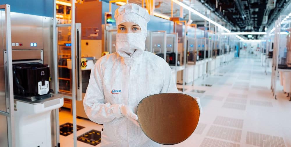
Photo: Anja Grabinger / Fraunhofer IISB