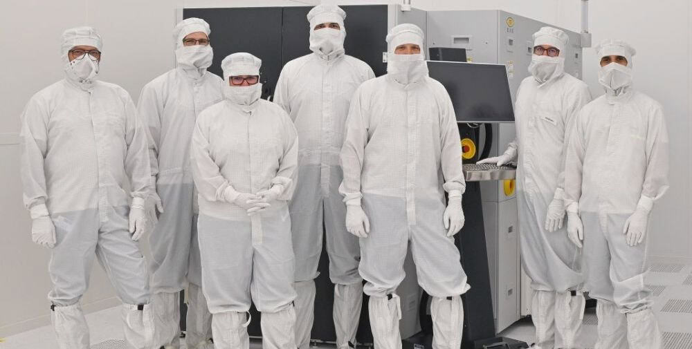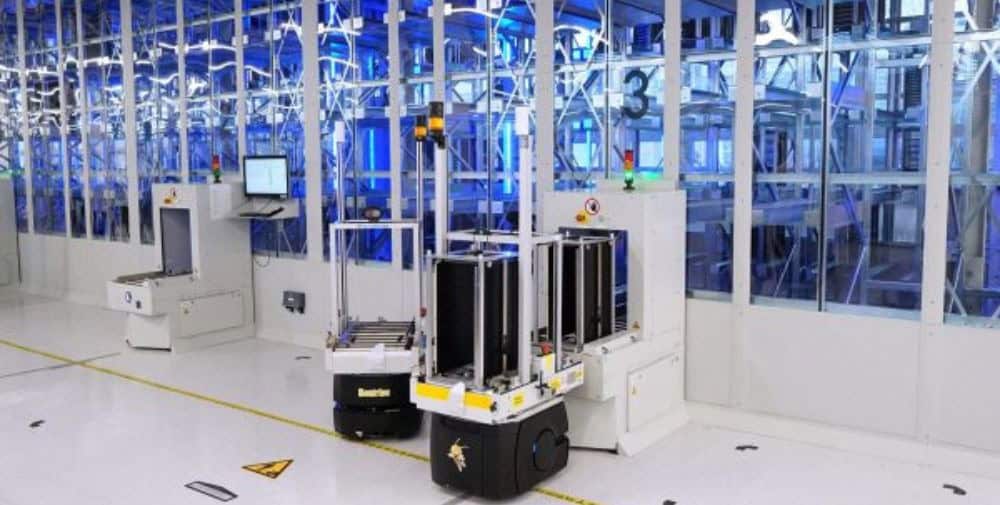
In its own laboratories and the 1500 m² clean room, the Fraunhofer Institute for Photonic Microsystems IPMS develops a wide variety of application-specific area light modulators based on 200 mm wafer technology. To enable individual deflection of each micromirror, a highly integrated electronic circuit (ASIC) is used as the basis for the component architecture. In combination with monolithically integrated MEMS (Micro Electro Mechanical Systems) technology, unique micromirror arrays are created. In addition, Fraunhofer IPMS develops the electronics and software to drive the devices. To facilitate the technology transfer into application, the institute offers evaluation kits to its customers. In addition to the micromirror chip itself, the ready-for-trial setup includes the complete control electronics including software.
The Fraunhofer IPMS area light modulators are used, for example, in microlithography in the deep ultraviolet range, in the manufacture of printed circuit boards (PCBs), in semiconductor inspection and metrology as well as in adaptive optics, astronomy, holography and microscopy. The research institute’s ISO 9001 certification underscores its quality, competence and performance.
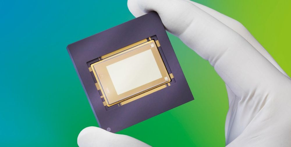
High-performance 2-axis tilting mirrors from Fraunhofer IPMS
A groundbreaking development of the Dresden-based research institute is the technology platform of a CMOS-integrated micromirror array in which each mirror can be individually deflected via two tilting axes. The device consists of 512 x 320 individually addressable mirrors with 48 μm pixel size and enables the redirection of light beams or the generation and control of 2D intensity profiles and patterns with variable intensity. Since light redistribution occurs instead of masking, high light efficiency is possible.
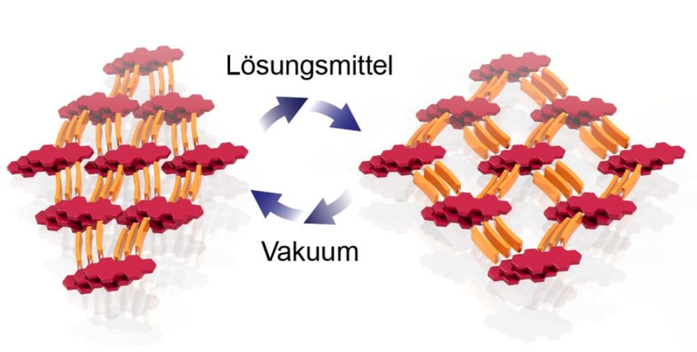
Strapezoidal mirror arrays for 3D holography
A new field of application for the Fraunhofer IPMS’s trapezoidal mirrors is holography. Holographic projection enables the spatial virtual representation of objects with a 3D observer experience, identical to that for real objects, in contrast to alternative methods such as stereo projection.
In the future, Fraunhofer IPMS micromirror arrays will enable computer-generated holography. Real and virtual worlds merge – moving and in real time. A mirror matrix optimized for holography is currently under development. The first application scenario addressed here is an automotive head-up display (HUD) (more in our virtual showroom).
At the Photonix trade show in Japan from October 4 to 6, visitors can examine the latest developments from Fraunhofer IPMS. A 2-axis tilting mirror demonstrator will be presented. In addition, the technology of area light modulators will be explained using macro models. The Fraunhofer IPMS booth is located at Makuhari Messe (Chiba, Greater Tokyo Area) in Hall 8 Booth #49-10. For an expert talk, appointments with scientists and developers can be made in advance via the Fraunhofer IPMS website).
About Fraunhofer IPMS
The Fraunhofer Institute for Photonic Microsystems IPMS stands for applied research and development in the fields of smart industrial solutions and manufacturing, medical technology and health, and mobility. Research focuses on miniaturized sensors and actuators, integrated circuits, wireless and wired data communication, and customized MEMS systems.
In two state-of-the-art clean rooms, research and development takes place on 200 and 300 mm wafers. Services range from conceptual design and process development to pilot series production.
– – –
Further links
👉 www.ipms.fraunhofer.de
Photo: Fraunhofer IPMS
.