X-FAB Dresden: Interview with Rico Tillner, Managing Director
How does X-FAB Dresden view the location? What role does the Saxon microelectronics network play for the company? Where does joint location work end and competition begin? Which prerequisites are absolutely necessary for future growth? You can find out all this and much more in the interview with Rico Tillner.
Mr. Tillner, what is the importance of the Dresden site for the group?
X-FAB produces at six different sites worldwide. Each location has its own technology portfolio. Of course, there are overlaps and redundancies for individual technologies, but no two sites are alike. Dresden is one of only two locations where our 350nm technology, which is very important for the automotive industry, is manufactured. In addition, the Dresden site is the only one within the X-FAB group to develop a gallium nitride technology together with our customers.
In which specific areas have investments been made since the opening and how high were these investments in total?
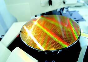
Due to its long history, the site has already experienced many changes. Production was started with 5-inch wafers and switched to 6-inch wafers in 2001. Since 2014, we have been manufacturing exclusively on 8-inch wafers. Regular investments have been made in the current production capacity in recent years, also with the help of funding projects such as IPCEI. Since the start of the switch to 8-inch wafers, more than 100 million euros have been invested. We will continue to invest in the modernization and expansion of the site.
For what uses does the Dresden site produce? What exactly can the chips produced and in which sectors / industries they are used?
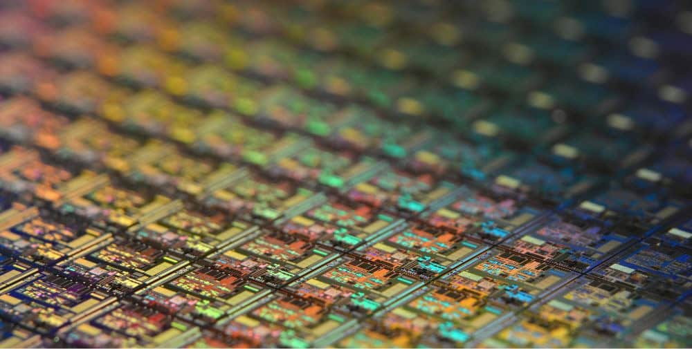
More than half, the chips produced in Dresden, is used in the automotive industry. The applications are very diverse and range from vehicle control, level measurement to lighting and locking systems. Furthermore, we produce chips for medical technology, mostly in connection with our MEMS factories in Erfurt and Itzehoe. These circuits are used, for example, for infrared temperature measurement. Other applications are so-called lab-on-a-chip circuits, which can be used for the selection of cancer cells or for drug tests on living cells.
There are now five fabs, numerous supplier companies and research institutions as well as microelectronics-related software companies in Saxony. In which areas is the network particularly important for your company?
The network in Dresden plays a very important role for us. On the one hand, we benefit very much from the short distances to many of our equipment manufacturers and suppliers. This helps us to be able to react quickly in case of problems and enables on-site support without long travel times. Furthermore, in the field of automation and analytics, for example, there are very good partners within the network with whom we cooperate.
Are there concrete cooperation projects here with other players at the site and if so, which ones?
Cooperations exist, for example, within the framework of funded projects regularly with various Fraunhofer institutes or other research institutions. In addition, we also cooperate with the Fraunhofer institutes in the field of development and production and use here mutually the respective available technical possibilities.
The topic of skilled workers not only moves us. Currently, Saxony’s ICT sector is growing by around 5,000 skilled workers per year, which equates to over 100,000 skilled workers in 2030 if growth remains constant. What role does direct proximity to other fabs play in the context of your skilled workers strategy? Does it make the location more attractive or the competition greater?
In the end, it is both. A location like Dresden with this concentration of different companies in the field of microelectronics is unique in Europe. This has an attraction beyond Saxony and leads to skilled workers coming to the region. But of course, the competition at the location also increases the competition for talent. You have to face up to this competition. To do this, it is important to know one’s strengths and to use them. Every factory has its individual strengths and it is important to find exactly the skilled workers who are looking for them. Our factory is the smallest on the site. This allows us to have a very familiar working environment and flat hierarchies. We also offer our employees very flexible development opportunities based on their interests.
Intel is planning a so-called mega-fab with Magdeburger? What impact will this have on you with regard to supply chains, service providers, raw materials and also skilled workers?
Microelectronics is a very complex industry that relies on very many different and highly specialized raw materials (wafers, chemicals, gases). We need a sufficiently large number of semiconductor factories in Europe so that investments in the production of the required raw materials are also worthwhile. Otherwise, additional dependencies will arise in other regions of the world. For this reason, the settlement of Intel is for me a positive sign to strengthen the location.
What is your vision for the location? How would you like to develop this further?
In my opinion, it is important for the location that the focus is not only on lighthouse projects and the latest and smallest technologies, but that the location grows in breadth. The value chains in microelectronics are long and very diverse. In the end, many different processes are necessary before a circuit can fulfill its task in a car, for example. As a technology location, this range should be covered in both research and production, and should also be supported politically. Ultimately, a high degree of diversification is a basic prerequisite for a high degree of economic stability, even in times of crisis.
What are concrete support measures that are necessary on the way to this vision?
Support programs have a high priority for microelectronics, especially in view of global competition. Here it would be desirable that the programs are defined as concretely as possible and designed unbureaucratically. Most important, however, is that a funding rate can be achieved that is comparable with those of other countries worldwide.
In terms of skilled labor strategies, further measures are needed to achieve more degrees in STEM professions. By this I mean not only degrees, but also vocational training in these fields. Initiatives are needed here to get young people from all areas of society interested in STEM professions as early as possible. In particular, programs to reach girls and young women more effectively for these professions must be expanded. But simply training or retraining new skilled workers will not be enough if the site is to continue to grow strongly. Policymakers should continue to work on improving the attractiveness of the location for foreign skilled workers, reducing bureaucratic hurdles and facilitating integration. Thank you very much for the interview, Mr. Tillner.
This interview was first published as part of our magazine NEXT “In Focus: Microelectronics”.
To the complete issue of the magazine.
More interviews in this series:
Infineon Dresden: Interview with Raik Brettschneider, Vice President & Managing Director.
GlobalFoundries: Interview with Dr. Manfred Horstmann, Sr. Vice President & General Manager
SAW COMPONENTS: Interview with Frieder Birkholz, General Manager
Robert Bosch Semiconductor Manufacturing Dresden: Interview with Dr. Christian Koitzsch, Plant Manager
Further links:
Saxony’s chip industry strengthens its supply chains.
Germany’s Microelectronics Landscape – The Semiconductor Heart of Europe Beats Here
European Chips Act: Good, but good enough?