The main idea of his work is to use automated model refinement for integrated circuit design to incorporate and understand problematic effects. This is accomplished via targeted changes to parameters and structures that allow previously unknown information about an integrated circuit to be found, merged and used to improve the circuit design. All methods have been tested in chip developments at IMMS. The results are used and followed up in various research and industry-driven chip design projects and are the basis for the AI-based design and test automation researched at IMMS.
Simulation and verification of analog and analog-digital integrated circuits shaped by empirical knowledge
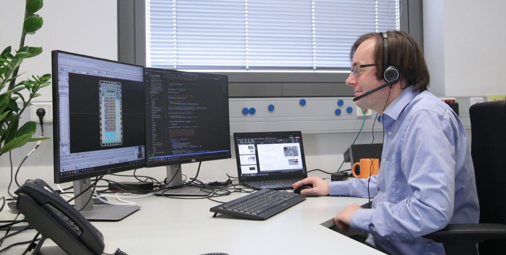
“In chip design, problems often come to light very late – for example, not until the layout, i.e. the blueprint that is ultimately developed for manufacturing. Then, in extreme cases, you suddenly discover that, for example, lines are too close together and can impair performance due to crosstalk or, in combination with other effects, even destroy a chip,” explains Georg Gläser. In order to work through error causes from the individual transistor, of which there can be millions in a circuit, to the complex overall system design level by design level, it takes a lot of time, since all these levels have to be described and simulated in detail with models, Georg Gläser continues. “The main problem, however, is that the models have so far not been able to show many effects at all. This is because people often work with simplified macro models that usually do not represent noise, parasitic couplings or unfavorable effects of deeper design levels.” Up to now, only experience has helped. Existing methods also usually start at only one design level. In addition, the systems and thus the simulations required for them are becoming increasingly complex, as more and more functionality and thus circuit elements are to be accommodated on ever smaller chip areas, if possible.
Methods provide more knowledge about the circuit and reduce design costs
On the one hand, the methods make it possible to integrate disturbing effects into the models in order to be able to represent them in more complex simulation scenarios. On the other hand, they provide insights into where the models, circuits and systems work and where they do not. In addition, the methods make it possible to estimate design uncertainties early on and reduce iterations in the design and thus costs. For example, one method, symmetry search for parasitic elements, yielded 223 possible problem locations as results for the development of a contact image sensor chip at IMMS after only 6 hours of computation, which otherwise would have had to be found by hand. Another method for identifying problematic couplings in the layout was already successfully used industrially by partners of the IMMS before the dissertation was published.
In the dissertation, five methods are presented that can be used at each design level or at the transition to the next. This is a distinct advantage over other work, which is usually limited to one level in the design process. As an example, some are described here.
Invasive analysis for early detection of previously unconsidered effects
In the work, invasive analysis can be used to dynamically adjust system models to gain insight into possible or existing perturbations, such as coupling of lines. The framework developed for this purpose, with several 10,000 lines of code, is suitable for very complex systems and can analyze the program code of behavioral models, adapt the models accordingly, and address the simulator. For example, parasitic elements are inserted or removed in this way, or test and observation modules are used.
Parasitic Symmetry Analysis and Acceptance Regions
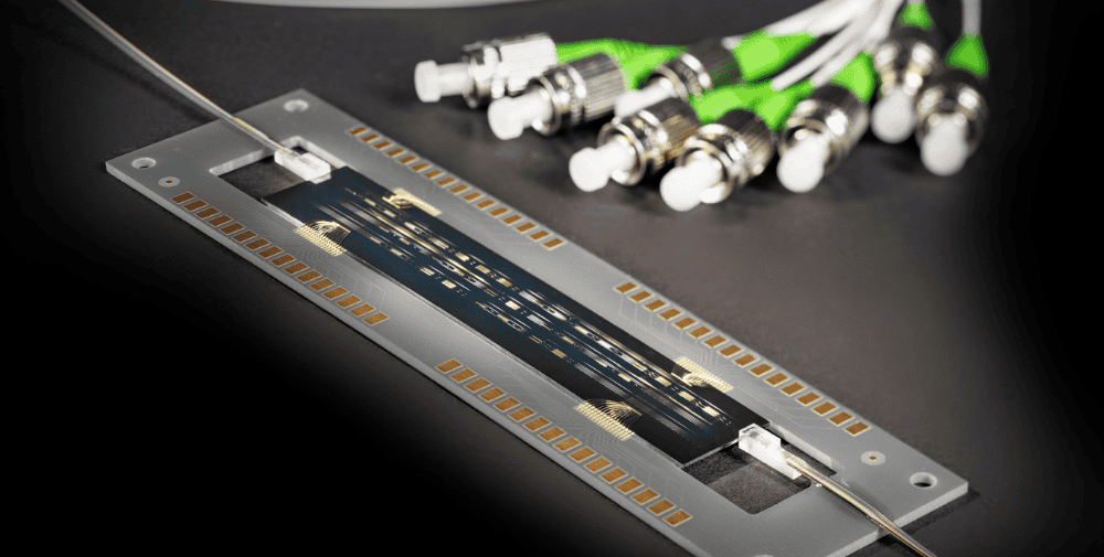
Many problems are often only visible in the layout, e.g. when couplings are created by closely spaced lines, allowing signal paths that result in undesired effects. Up to now, layout troubleshooting is done by trial and error with many manual simulations to find out where the error comes from, sometimes also with statistical methods. A systematic for the analysis of mixed-signal systems before layout was missing.
The starting point of the new approach to symmetry analysis is that symmetry is a core concept in circuit design itself. The idea is to find interfering operating conditions that are symmetrical, and therefore cancel each other out, and thus can be eliminated from further troubleshooting, similar to Active Noise Cancelling headphones that can cancel noise with exactly opposite signals of the same strength so that it is no longer perceived as annoying.
In order to be able to map and analyze these disturbance variables, which are not present in the circuit diagram, nevertheless with the method, the method of the acceptance regions is used. With it, symmetries can be made visible and derived as a basis for the search algorithm. Behind this are complex algorithms that examine all possible symmetry pairs with maximum values. The method classifies the parameter space into segments that show where the system works and where it does not. The advantage of the method is that it is not necessary to know the layout.
Foundation for the research of AI-based design and test automation at IMMS
That the work is an important contribution on the way to further design automation of analog and mixed-signal circuits, opens up new optimization potentials in circuit design, and significantly expands the state of the art in EDA, was already attested to Georg Gläser when he received the EDA Achievement Award by the edacentrum long before he submitted his dissertation. Prof. Dr.-Ing. Ralf Sommer could endorse this without reservation. Georg Gläser’s doctoral supervisor and scientific director of the IMMS as well as head of the Department of Electronic Circuits and Systems at the Faculty of Electrical Engineering and Information Technology at the Ilmenau University of Technology added: “Georg Gläser’s methods also set the course for research into AI-based design and test automation at the IMMS, which he has played a key role in shaping and for which he has systematically built up a team of experts in recent years in order to further advance the subject.” He also said that under his leadership, research groups and projects had been acquired and worked on to expand know-how in this field, and that on this basis a range of services had been established to provide methodological support to industrial customers. In addition, he has initiated further dissertations in the field within his team, which are very promising, Sommer added. “We are excited about what the future holds. Georg Gläser has made a great contribution of which we are very proud.”
About IMMS Institut für Mikroelektronik- und Mechatronik-Systeme gemeinnützige GmbH (IMMS GmbH)
The IMMS supports companies in launching internationally successful innovations for health, the environment and industry and accompanies them from the feasibility study to series production. It advances companies with application-oriented research and development in microelectronics, systems engineering and mechatronics and transfers results of basic research into applications. The IMMS was founded in 1995 as a state-owned enterprise of the Free State of Thuringia and is an affiliated institute of the TU Ilmenau. It operates with a team of about 90 people at its headquarters in Ilmenau and at the institute’s branch in Erfurt.
Further links
www.imms.de
Photo: IMMS