Contactless monitoring of lamination temperature enables self-optimizing process control in printed circuit board manufacturing.
Categories
Contactless monitoring of lamination temperature enables self-optimizing process control in printed circuit board manufacturing.
Categories
Tags
Contact info
Silicon Saxony
Marketing, Kommunikation und Öffentlichkeitsarbeit
Manfred-von-Ardenne-Ring 20 F
Fax: +49 351 8925 889
Contact person:
Rotte GmbH and Fraunhofer ENAS show how sensors can optimize production even under harsh conditions. Together they developed a contactless temperature measurement system for permanent monitoring of the laminating temperature of an automatic pressing process. Self-learning and -optimizing process control can, for example, reduce process times. Efficiency increases of up to 25% are expected to be achieved.
In printed circuit board manufacturing, multilayer printed circuit boards are produced by laminating prepreg layers sequentially onto a preprocessed printed circuit board core. Up to 20 such core/prepreg layers are stacked cost-efficiently in a pile (book) manually on workpiece carriers and then transported via a conveyor system to multi-daylight heating presses. There they are laminated together with other tool carriers. This process takes place in a vacuum chamber where the book is pressed between two heating plates for 80-90 minutes. Because the book is thick, the outer layers heat up faster than the inner layers. To ensure that all layers are pressed for a sufficiently long time and heated to the correct temperature, this is currently done by controlling the temperature of the heating plates and setting the pressing time based on empirical values.
For optimal process control and documentation, it is fundamentally necessary to continuously measure the core temperature of the PCB book. However, such a measurement currently has a significant impact on the manufacturing process.
Temperature sensors are inserted into the various layers during manual stacking of the book. These sensors must then be manually connected to corresponding contacts in the vacuum chamber, which requires an interruption of the automatic production process. This interruption leads to a high production loss, which is why such measurements can only be carried out sporadically and not regularly.
As part of the project, a contactless method was developed that allows the sensors to be read out, thus avoiding manual intervention in the ongoing production process. The availability of such a system represents a significant advance, as permanent process control is made possible in the automated production sequence.
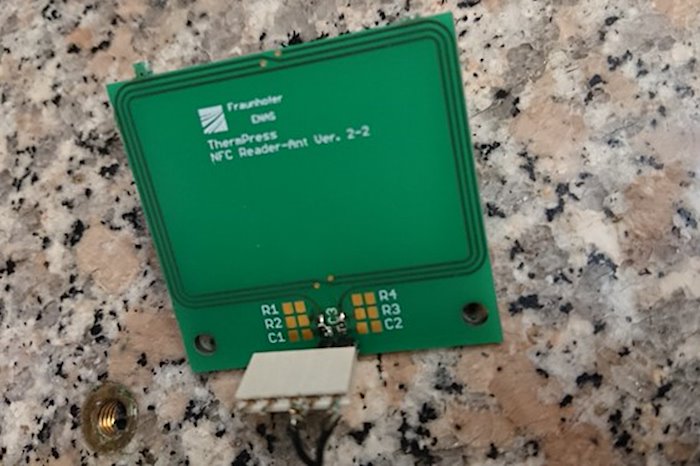
Reader antenna | Image: Fraunhofer ENAS
In the future, the laminates can be prepared directly at the laying stations in the logistics process. The prepared workpiece carriers can then send their recorded measurement data to the process controller in the laminating press without further manual intervention to ensure laminate quality.
Likewise, the field-proven process can be used for the production of other technical laminates.
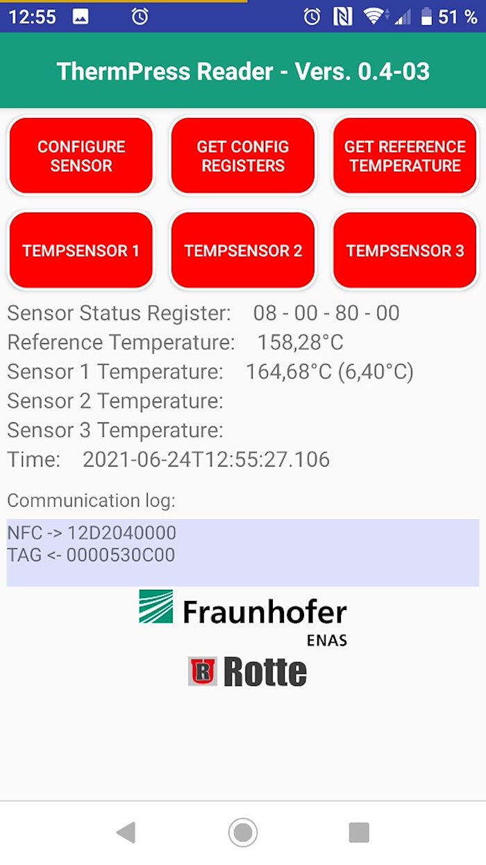
Graphical user interface for reading the sensor via NFC smartphone | Image: Fraunhofer ENAS
_ _ _ _ _

Dr. Alexander Weiß
Head of Business Unit “Intelligent Sensor and Actuator Systems
E-mail: alexander.weiss@enas.fraunhofer.de
_ _ _ _ _
The particular strength of the Fraunhofer Institute for Electronic Nano Systems ENAS lies in the development of smart integrated systems for different applications. Fraunhofer ENAS develops single components, technologies for their manufacturing as well as system concepts and system integration technologies and transfers them into production. The institute offers research and development services from the idea, via design and technology development or realization based on established technologies up to tested prototypes.
Fraunhofer Institute for Electronic Nano Systems ENAS
Technology Campus 3
09126 Chemnitz
Phone: +49 371 45001-0