Graphene has the potential for exceptional performance in applications ranging from solar cells, organic light-emitting diodes (OLEDs), electrical energy storage devices and smart windows to membranes, e.g. for seawater desalination. Its outstanding properties are impressive: the material is transparent, lightweight and stronger than steel. Graphene also has a high conductivity for heat and electricity and is very flexible.
Researchers have been working for several years on the integration of graphene as a transparent electrode in photovoltaics or in OLEDs, e.g. for curved touchscreens or to increase the efficiency of solar cells. Thanks to its high electrical conductivity, graphene can contribute to faster charging and discharging cycles in energy storage devices such as batteries or supercapacitors. Its large surface area also enables a higher capacity and energy density, while the mechanical stability of the material contributes to the service life and reliability of such storage devices.
So far, the scalability of depositing graphene with consistently high quality has limited its use. In addition, the integration of graphene into existing manufacturing processes poses a technical challenge.
The Fraunhofer FEP has more than 30 years of expertise in the development of customized layers and layer systems. With its core competencies in electron beam and plasma technology as well as in process development for the deposition of homogeneous, thin layers, e.g. in roll-to-roll processes, the researchers are working on a new technology for the synthesis of graphene using PECVD (Plasma Enhanced Chemical Vapor Deposition). The first important foundations for future cost-efficient graphene deposition processes have now been laid within the funded EU project NewSkin (FKZ 862100).
Plasma process for more efficient production of graphene
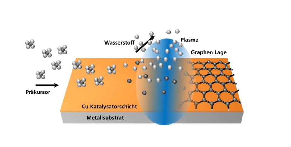
Current synthesis processes for graphene require the use of high temperatures and catalysts. The scientists at Fraunhofer FEP, on the other hand, use plasma-assisted processes. This allows the parameter window for the production of graphene to be significantly expanded, so that deposition is also possible at lower substrate temperatures and higher throughputs.
The researchers at Fraunhofer FEP used the versatility of the MAXI inline coating system to develop the new process. Depending on the development maturity of the process, the multifunctional vacuum system offers the possibility of carrying out processes both in sheet-to-sheet mode and in roll-to-roll mode. The variety of processes extends to pilot production, making the system a good basis for the development and scaling of processes for the deposition of graphene.
Dr. Stefan Saager, Group Manager for Coating Metal and Energy Technology, explains the technology: “The PECVD process developed can be used to deposit graphene on metallic strips. The roll-to-roll mode of the MAXI system is used for this. In the first step, the metal strip is coated with a thin layer of a catalyst material such as copper in a vacuum. This allows the desired substrate material to be selected independently of the suitable catalyst material. Immediately afterwards, the coated metal strip is moved into a process unit with an argon plasma discharge. The argon ions generated there collide with the substrate and heat it highly efficiently in a very short time. By adding a suitable precursor gas such as methane or acetylene in the immediate vicinity of the plasma discharge, the respective molecules can be broken down into their individual components and partially ionized at the same time. Ideally, the carbon atoms and ions generated in this process are deposited on the substrate in a single-layer, ordered 2D structure, thus creating the desired layer of graphene.”
By supporting the ions present in the plasma, the formation process can be realized at comparatively lower substrate temperatures than was previously possible with other state-of-the-art processes.
Researchers at Fraunhofer FEP have already been able to synthesize graphene with the newly developed PECVD process over a width of 280 mm at process speeds of one meter per minute. The process thus enables high production throughputs and the associated cost savings for future production processes. In addition, the technology allows an expansion of the substrate materials that can be used and thus a broader range of applications.
Reproducibility and optimization on the agenda
In the next step, the scientists at Fraunhofer FEP are working on the reproducibility of the results and on further improving the layer properties achieved, e.g. with regard to the number of graphene layers.
Another challenge of the new technology development lies in the precise control of the plasma and temperature conditions for uniform layer qualities and morphologies. In addition, future research will focus on improving the winding process of the hot ribbon and on further scaling the existing process parameters.
With the results achieved, the existing know-how and the plant equipment, the Fraunhofer FEP offers manufacturers from the electronics and renewable energy sectors as well as other technology companies and research institutions a basis for projects for the further development and scaling of processes for the synthesis of graphene.
– – – – – –
Further links
👉 www.fep.fraunhofer.de
Photo: Fraunhofer FEP
