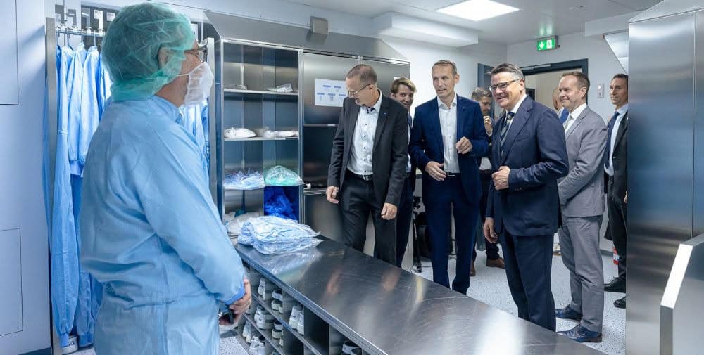
“The semiconductor industry is of central importance for almost all future technologies – from autonomous driving to artificial intelligence. The fact that a company like ZEISS is investing in Hesse is a strong sign for our business location,” says Hesse’s Minister President Boris Rhein. He took part in a small opening ceremony in Roßdorf on September 17, 2025 and also took the opportunity to visit the site. Around 280 employees of the strategic business unit ZEISS Semiconductor Mask Solutions (SMS) are employed in Roßdorf
Space for growth and new tools
With the new cleanrooms, ZEISS SMT is not only creating optimal conditions for precision work in the nanometer range – clean, vibration-free and controlled – but also urgently needed space: The expansion offers space for four additional tools, highly specialized systems that enable the production of defect-free high-end photomasks. “The commissioning is a milestone for our business unit,” says Dr. Clemens Neuenhahn, Head of ZEISS SMS. “We are specifically expanding our research and development capacities in order to meet the increasing technological complexity in mask repair. ZEISS has a tradition of investing in research and infrastructure – this is a key prerequisite for remaining a technology leader in the future.” Roßdorf has been a ZEISS SMT site since 2005, when ZEISS acquired NaWoTec GmbH, a spin-off of Deutsche Telekom. “Our team has grown considerably over the past 20 years: in 2015 we had around 80 employees, today we have around 280. This development shows what is possible with start-up DNA, the backing of a global technology group and the tech ecosystem around Darmstadt,” says Dr. Patrick Villwock, Head of Development and Site Manager at ZEISS SMT in Rossdorf.
Location with many advantages
Rossdorf offers several advantages as a location: Its location in the Rhine-Main metropolitan region ensures excellent transport connections – with Frankfurt Airport as an international logistics and travel hub. The proximity to the science city of Darmstadt, its technical university and research facilities is also a decisive advantage. ZEISS maintains intensive networks with students and teachers and benefits from its proximity to academic talent. There is also a research cooperation with the ZEISS Innovation Hub @ KIT in Karlsruhe – an interdisciplinary development center at the interface between science and industry.
Precision for the semiconductor industry
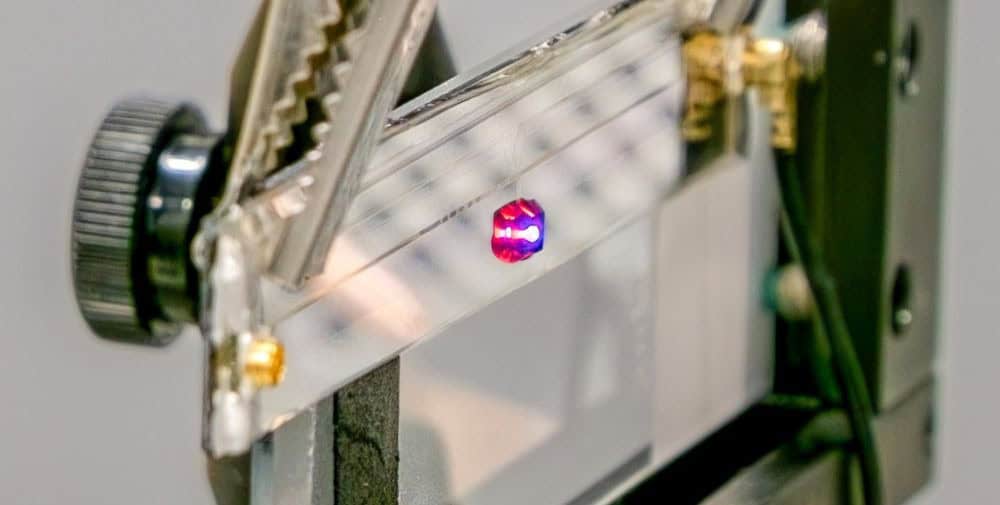
Photomasks are used in microchip production as optical templates to expose the finest nanostructures on silicon wafers – comparable to an extremely precise slide. Even the smallest defects on these masks can lead to rejects and thus impair the quality and efficiency of production. The MERiT® systems from ZEISS SMT developed at the Roßdorf site eliminate such defects without contact, using electron beam technology and nanometer precision – without damaging the masks. They help to ensure production yields and guarantee the quality of modern microchips. All major semiconductor manufacturers worldwide use ZEISS SMT systems to reliably repair photomasks. Because microchips are becoming ever smaller, more powerful and more energy-efficient, the demands on the repair processes are also increasing. This is why the technology in Roßdorf is being continuously developed further.
About ZEISS
ZEISS is a leading global technology company in the optical and optoelectronic industry. In its four divisions Semiconductor Manufacturing Technology, Industrial Quality & Research, Medical Technology and Consumer Markets, the ZEISS Group most recently generated annual sales of around 11 billion euros (September 30, 2024).
ZEISS develops, produces and distributes highly innovative solutions for industrial metrology and quality assurance, microscopy solutions for life sciences and materials research, and medical technology solutions for diagnostics and therapy in ophthalmology and microsurgery for its customers. ZEISS also stands for the world’s leading lithography optics, which are used by the chip industry to manufacture semiconductor components. ZEISS branded products such as ophthalmic lenses, photographic lenses and binoculars are sought-after and trendsetters worldwide.
With a portfolio geared towards future growth areas such as digitalization, health and Industry 4.0 and a strong brand, ZEISS is helping to shape technological progress and is advancing the world of optics and related areas with its solutions. The basis for the success and further continuous expansion of ZEISS’ technology and market leadership is the sustained high level of expenditure on research and development. ZEISS invests 14% of its revenue in research and development work – this high level of expenditure has a long tradition at ZEISS and is also an investment in the future.
With more than 46,555 employees, ZEISS is active in around 50 countries with more than 60 sales and service locations, around 40 research and development locations and 35 production sites worldwide (March 31, 2025). The headquarters of the company, which was founded in Jena in 1846, is located in Oberkochen, Germany. The sole owner of the parent company, Carl Zeiss AG, is the Carl Zeiss Foundation, one of the largest German foundations for the promotion of science.
Semiconductor Manufacturing Technology
With its product portfolio and world-leading expertise, the Semiconductor Manufacturing Technology division covers various key processes in the manufacture of microchips. The division’s products include semiconductor manufacturing optics – including lithography optics – photomask systems and process control solutions for the semiconductor industry. Thanks to ZEISS technologies, microchips are becoming increasingly smaller, more powerful, more energy-efficient and less expensive. The resulting electronic applications enable global progress in various disciplines, including technology, electronics, communications, entertainment, mobility and energy. Semiconductor Manufacturing Technology is headquartered in Oberkochen. Other locations of the division are Jena, Roßdorf, Wetzlar, Aachen and Coswig (Germany), Zurich (Switzerland) as well as Bar Lev (Israel) and Dublin (USA). ZEISS SMT also has various sales and service locations in the USA, China, Taiwan (region), South Korea and Japan.
– – – – –
Further links
👉 www.zeiss.de
Photo: ZEISS