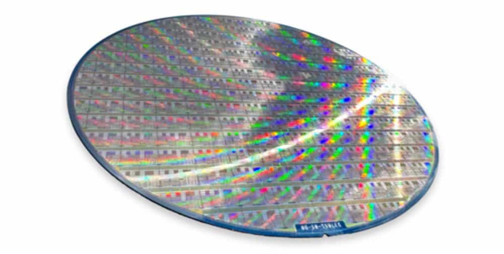
X-FAB offers GaN-on-Si technology from its state-of-the-art 8-inch fab in Dresden, Germany, one of six manufacturing facilities the company operates worldwide. The Dresden fab features a wide range of specialized processing equipment, metrology tools and technologies optimized for GaN and analog CMOS development and production in a stable, trusted and automotive-qualified factory environment. The on-site tooling has been optimized for processing the thicker GaN-on-Si wafers required by customers in sectors such as automotive, data centers, industrial, renewable energy, medical and others.
Thanks to its long-standing experience in high-voltage GaN, the company’s in-house expertise now extends to GaN-on-Si foundry services for dMode devices, following the recent release of XG035 dMode technology as an open foundry platform. The process includes dMode HEMT transistors (scalable from 100V to 650V), which are commonly used in power conversion applications. In addition, X-FAB offers custom GaN technologies including dMode, eMode HEMTs as well as Schottky barrier diodes, which are popular for high-frequency rectification, power supply and solar panel applications, among others.
Global demand is growing for charging applications, electric vehicles, advanced energy management systems and more powerful data centers. In terms of the latter, the training and use of AI is driving the need for more computing resources, resulting in higher power requirements and more efficient power supply and conversion.
GaN-on-Si technology is a promising semiconductor process that enables high switching frequency and low RDS (resistance between drain and source terminals) in the on state. With its small footprint and high dielectric strength, GaN-on-Si completes X-FAB’s offering for WBG chip processes and enables customers to develop products that improve energy efficiency from the power grid to the car battery or GPU.
“With over 30 years of experience in automotive CMOS technologies – including 350nm CMOS, common tool sets and common BEOL – our GaN offering provides integrated quality and significantly lower barriers to entry,” explains Michael Woittennek, CEO of X-FAB Dresden. “After many years of developing customized technologies, we are now opening our XG035 dMode technology for general prototyping projects in our Dresden factory – in the heart of Silicon Saxony. The flexibility of our 350nm tool set also allows us to quickly transition to volume production, providing our customers with a fast and reliable route to market.”
“With the changing landscape of GaN vendors, X-FAB is positioning itself as a dedicated GaN foundry partner,” added Luigi Di Capua, VP Product Marketing. “Our 8-inch GaN-on-Si platform helps customers secure their supply chain and scale their designs with confidence.”
A PDK that simplifies the design process for customers and enables faster onboarding is available. In addition, a public MPW shuttle service will be offered from Q4 2025, allowing multiple customers to share a single silicon wafer for chip manufacturing. These steps further lower the barriers to entry for prototype development and low-volume production.
– – – – –
Further links
👉 www.xfab.com
Photo: X-FAB