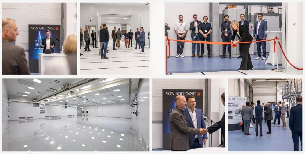
Semiconductor applications require new materials and new form factors to continue driving innovations and pushing technology boundaries. VON ARDENNE and the company’s process and material expertise are key to developing and introducing new materials and to supporting customers in their product development.
The cleanroom will be equipped first with a new OPTA X300 deposition system. It will be available from mid-2026 for joint material and device developments. VON ARDENNE will cover the entire process from simulating layers and their functions, through laboratory and pilot-scale sampling, to measuring and evaluating layer and device properties. This gives customers the opportunity to test the function of the coating for your product in a relevant environment in advance, including their process-chain.
Specifically precise optical coatings as well as materials used for piezoelectrical and memory materials are increasingly in demand. The new cleanroom with the installed equipment can help accelerate the development of such materials.
“We’re excited to collaborate with our partners in this cutting-edge environment and drive innovation in next-generation semiconductor applications”, says Sven Frauenstein, VP Semiconductors at VON ARDENNE.
– – – – – –
Further links
https://vonardenne.de/
Photos: VON ARDENNE