The three-year project, coordinated by CEA-Leti, brings together 58 partners from across the European semiconductor value chain, including large companies and subject matter experts (SMEs) as well as research institutes, universities and industry associations. GENESIS will drive innovative solutions in the areas of emission control, environmentally friendly materials such as alternatives to per- and polyfluorinated alkyl substances (PFAS), waste minimization and reuse of raw materials, which are directly aligned with the European Green Deal and the European Chips Act.
“The GENESIS partners are committed to working together fruitfully and constructively throughout the duration of the project to achieve a sustainable impact on the European semiconductor ecosystem,” said Laurent Pain, Director of the Sustainable Electronics Program at CEA-LETI and coordinator of the GENESIS project.
SEMI Europe will oversee the dissemination of information and promotion of activities to raise awareness and understanding of the importance of sustainable semiconductor manufacturing technologies in industry and academia.
SEMI “The European semiconductor industry recognizes the urgency of finding alternatives to materials of concern and reducing greenhouse gas emissions,” said Laith Altimime, President of SEMI Europe. “With the increasing demand for semiconductors, the European Commission is encouraging sustainable innovative solutions by funding important initiatives such as GENESIS.”
The GENESIS consortium will focus on scientific research during the three-year project period to facilitate the industry’s transition to sustainable manufacturing. In addition, the initiative will create added value through knowledge exchange, job creation and positive socio-economic impact in the European regions represented by the project partners.
45 sustainability innovations on four strategic pillars
Pain noted that the GENESIS project team expects to deliver approximately 45 sustainability-oriented innovations for the entire life cycle of semiconductors, aligned with four strategic pillars that form the technological basis for GENESIS’ vision for a green European semiconductor industry:
Pillar 1 – Monitoring and sensing: Real-time emission tracking, traceability and process feedback systems
Pillar 2 – New materials: PFAS-free chemicals and low global warming potential alternatives for advanced semiconductor processes
Pillar 3 – Waste minimization: Innovations in recycling (solvents, gases, slurries), reuse and sustainable substitutes
Pillar 4 – Reducing the need for critical raw materials: strategies to reduce dependence on critical raw materials and strengthen resource security.
In addition to these pillars, the project objectives form an overall framework that includes the use of sensor-integrated abatement systems to reduce PFAS and greenhouse gas emissions. It also aims to position Europe as a pioneer in the development of green semiconductor technologies by aligning supply chain practices with environmental regulations.
A green solution for Europe’s chip agenda
“The launch of the GENESIS project is an important step in aligning Europe’s semiconductor ambitions with its climate change commitments,” said Anton Chichkov, program manager at Chips Joint Undertaking (Chips JU), a public-private partnership established to strengthen the semiconductor industry in Europe by fostering collaboration between the EU, Member States and the private sector.
“As chips increasingly become the backbone of everything from AI to energy systems, their environmental footprint is also growing rapidly,” said Chichkov. “GENESIS is responding to this urgent challenge by advancing sustainable alternatives in the areas of materials, waste reduction and resource efficiency. With this initiative, Europe is not only investing in cleaner technologies, but also positioning itself as a global leader in green semiconductor manufacturing.”
The GENESIS project is co-funded with a budget of almost 55 million euros by the Chips Joint Undertaking of the European Commission, the participating EU Member States and the Swiss State Secretariat for Education, Research and Innovation (SERI).
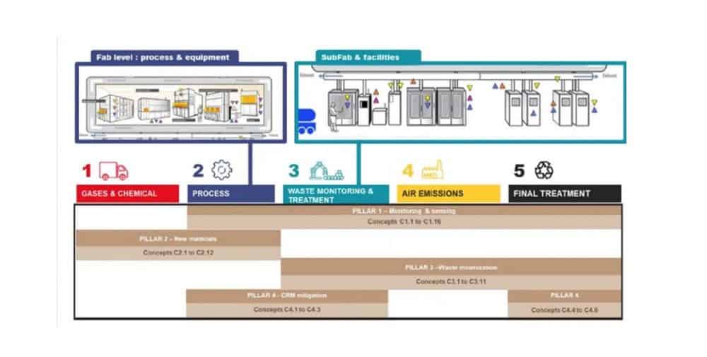
The five critical stages in the chip manufacturing lifecycle addressed by GENESIS
The GENESIS integrated roadmap outlines five critical stages in the semiconductor manufacturing lifecycle – materials (PFAS-free alternatives & gases and chemicals, processes, waste monitoring & treatment, air emissions and final treatment – where environmental impact can be minimized.
This structured approach guides the project’s efforts to reduce emissions, eliminate harmful substances and enable material recovery through innovations in sensing, materials, waste reduction and raw material reuse.
About GENESIS
GENESIS (GENErate a Sustainable Industry for Semiconductors) is a pan-European project co-funded by the EU, Chips JU, the Member States and the Swiss State Secretariat for Education, Research and Innovation (SERI). Coordinated by CEA-Leti, it involves 58 partners from across Europe focusing on moving semiconductor manufacturing towards a circular economy model aimed at minimizing waste and maximizing resource reuse and a low impact, innovation-driven industry.
About SEMI
SEMI® is a global industry association connecting over 3,000 member companies and 1.5 million professionals from across the semiconductor and electronics design and manufacturing supply chain worldwide. We foster collaboration among our members to address key industry challenges through advocacy, workforce development, sustainability, supply chain management and other programs. Our SEMICON® trade shows and events, technology communities, standards and market intelligence contribute to our members’ growth and innovation in design, devices, equipment, materials, services and software, enabling smarter, faster and safer electronics.
– – – – – –
Further links
👉 www.semi.org
👉 www.genesiseu.eu
Graphic: SEMI