“With this expansion, Okmetic strengthens its position as an EU-based full-line supplier for 150 to 200 mm silicon wafer platforms for the MEMS, sensor, RF and power markets. Increasing capacity for 200mm polished wafers strengthens long-term supply stability for critical semiconductor applications,” says President and CEO Kai Seikku.
The first wafers from the fab expansion were produced in June 2025, marking the beginning of a structured qualification and ramp phase. With volume production now underway in early 2026, Okmetic will deliver wafers from the expanded capacity to customers, strengthening long-term supply readiness for MEMS, RF, power and GaN-based applications.
The expansion builds on previous investments to increase capacity and strengthen the supply of silicon wafers in Europe
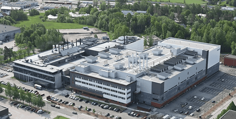
Vantaa site The fab expansion is expected to more than double Okmetic’s capacity by 2030. Construction of the expansion began in early 2023 and covers an area of over 40,000 m², including a 6,000 m² clean room area and areas for crystal growing and wafer production. The fab expansion is equipped with state-of-the-art technology, with a focus on energy efficiency.
Building on previous investments, Okmetic has significantly expanded its manufacturing capabilities in recent years, including doubling its production capacity for bonded SOI between 2017 and 2021 and adding a patterning line for cavity SOI production (C-SOI®) in 2019.
This latest expansion strengthens Okmetic’s ability to meet the changing needs of the semiconductor industry. By significantly increasing its 200mm polished wafer capacity, Okmetic solidifies its position as the leading European-based supplier of advanced silicon wafers and ensures a stable and high-quality supply of 150-200mm wafers.
About Okmetic
Founded in 1985, Okmetic is the leading supplier of advanced, high value-added silicon wafers for the manufacture of MEMS, sensor, RF and power devices. Okmetic has the broadest portfolio of 150 to 200 mm wafers on the market. It includes MEMS, RFSi® and power wafer product lines, including polished wafers, bonded silicon-on-insulator (SOI) wafers with or without cavities, patterned wafers and TSV wafers.
Okmetic’s headquarters are located in Vantaa, Finland, where the majority of the company’s silicon wafers are manufactured. A global sales organization and technical support ensure fast local service, rapid prototype development and highly optimized wafer solutions. Okmetic’s operations are based on quality and environmental management systems according to ISO 9001:2015, ISO 14001:2015 and IATF 16949:2016 standards.
Contact
President and CEO Kai Seikku
Email: kai.seikku@okmetic.com
– – – – – –
Further links
👉 www.okmetic.com
Photo: Okmetic