Company type
Home | Mitglieder |
SENTECH Instruments GmbH
Medium-sized companies (<250 employees or <50 million annual turnover)
Target markets
Electronics
Industries
Production·Technology
Portfolio
ALD·Atomic Layer Deposition (ALD)·Customized Solutions·ellipsometer·Equipment·Measurement Technology·Micro- / Nanoelektronics·Plasma Deposition·plasma etcher·Plasma Etching·Semiconductor Industry·Thin Film Metrology·thinfilm measurement
Certificates
Contact
Schwarzschildstraße 2
12489 Berlin
12489 Berlin
+49 30 6392 55-20
Contact Person
Friedrich P. Witek
+49 30 63 92 5530
Geschäftsführer
About this member
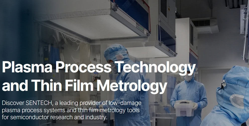
SENTECH is home to experts in plasma process technology and thin film metrology
SENTECH has over thirty years’ experience in developing, manufacturing, and marketing innovative capital equipment worldwide for the Research & Development and Industrial Production communities. Our robust systems focus on thin film deposition, patterning, and characterisation in semiconductor technology, microsystems technology, photovoltaics, nanotechnology, and materials research.
SENTECH Instruments, based in Berlin-Adlershof, was founded in 1990. All our systems and tools are developed, manufactured, and shipped worldwide from our Berlin site. Our teams of application, research and development, technical service, and sales experts are located in Berlin. SENTECH is continuously working to expand its product portfolio and global sales and service network. The company has experienced significant growth in recent years and now employs over 120 people. To meet the increasing customer demand for our systems, we invested in expanding our production capacities by adding a new building on our campus at the Berlin-Adlershof Technology Park, completed in 2020.
SENTECH Gesellschaft für Sensortechnik, based in Krailling near Munich, was founded in 1986 and provides sales representation for SENTECH across Germany and parts of Europe.
SENTECH SI 500 ICP-RIE
The SENTECH SI 500 ICP-RIE System represents the leading edge for ICP processing in both research and industry. The system comprises the ICP plasma source PTSA, a dynamic temperature-controlled substrate electrode, a fully controlled vacuum system, and a very easy-to-operate user interface. Configurations for processing a variety of materials, including but not limited to III-V and II-VI compound semiconductors (GaAs, InP, GaN, InSb), dielectrics, quartz, glass, silicon, silicon compounds (SiC, SiGe), and metals, are achievable with this flexible and modular plasma etch system. The versatile and modular system can be configured for ALE, cryo, DRIE, RIE plus for multi-wafers and large substrates.
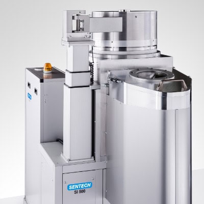
SENTECH SI 500 ICP-RIE Plasma Etching System
SENTECH SI 500 D ICPECVD System
The SENTECH SI 500 D ICPECVD System represents the leading edge for inductively coupled plasma (ICP) processing in both research and industry for plasma-enhanced chemical vapour deposition of dielectric films, a-Si, SiC, and other materials. The system comprises the ICP plasma source PTSA, a dynamic temperature-controlled substrate electrode, and a fully controlled vacuum system. A large variety of substrates from 100 mm wafers up to 200 mm diameter, as well as substrates on carriers, can be handled by the flexible load lock built into the SENTECH SI 500 D. The single-wafer vacuum load lock and mechanical clamping guarantee stable conditions and allow for straightforward switching of processes.
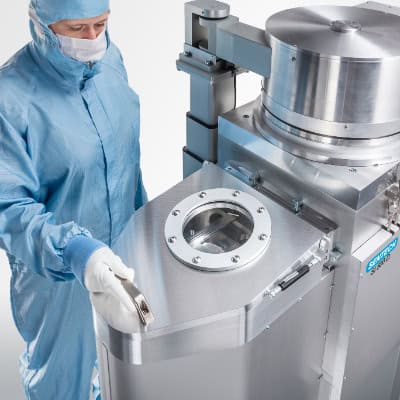
SENTECH SI 500 D ICPECVD Plasma Deposition System
SENTECH SI PEALD
SENTECH ALD Systems enable thermal and plasma-enhanced operation. Our ALD systems can be configured for oxide, nitride, 2D material deposition. 3D structures can be homogenously and conformally coated. With ALD, PECVD, and ICPECVD, SENTECH offers plasma deposition technology for depositing films from the nanometer scale up to several microns.
In-situ diagnostics by the AL Real Time Monitor enable ultra-high resolution of single ALD cycles. The advantages are confirmation of the ALD regime, reduction of process time, and total cost of ownership. Spectroscopic ellipsometry is provided as in-situ diagnostics, too, having specific advantages for our atomic layer deposition systems.
SENTECH SI PEALD
SENTECH Cluster System
SENTECH Cluster Systems comprise plasma etch and/or deposition modules, a transfer chamber, and a vacuum load lock or cassette station. Transfer chambers, including handling robot are available with three to six ports. Up to two cassette stations can be used to increase the throughput. SENTECH Cluster Configurations can be used to process a large variety of substrates from 100 mm wafers up to 200 mm in diameter. The systems offer different levels of automation, ranging from vacuum cassette loading to a one-process chamber for up to a six-port cluster configuration, with different etch and deposition modules offering high flexibility and high throughput. All SENTECH Cluster Systems are controlled by advanced hardware and SIA operating software, with a client-server architecture. A well-proven, reliable programmable logic controller (PLC) is used for the real-time control of all components.
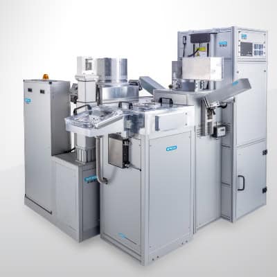
SENTECH Cluster System
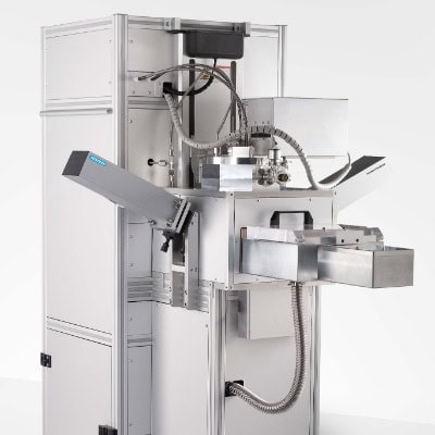
SENTECH SENDURO accuva10
The SENTECH SENDURO accuva10 is a fully automated thin film quality control tool housed in a compact > 2 m² footprint, making it ideal for research or production cleanroom environments. It is a measurement tool for quality control in sensors, RF/power devices, SAW filters, and MEMS production. The tool provides reliable and precise measurement of thin film stacks, using spectroscopic reflectometry and ellipsometry. Wafers are loaded from standard cassettes, and recipes carry out the quality control measurements. The tool is designed to measure film thicknesses, control deposition processes by measuring refractive indices of thin films, and prepare surface trimming for filters.
The system offers the configuration flexibility to meet the requirements of production control and QC. The tool can be configured with µ-spot measurements in reflectometry and ellipsometry, and pattern recognition, which provides an accurate measurement location. All measurements can be combined with edge-grip technology.
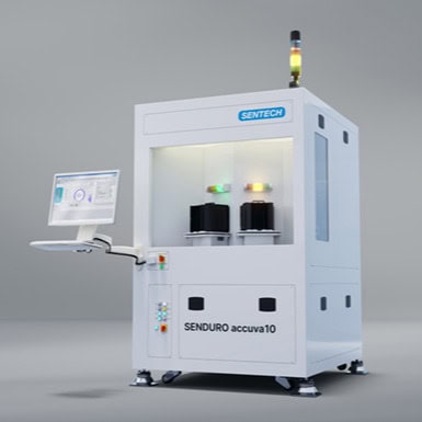
SENTECH SENDURO accuva10
SENTECH SENresearch 4.0
The SENTECH SENresearch 4.0 uses fast FTIR ellipsometry for the NIR up to 2,500 nm or 3,500 nm, respectively. It provides the broadest spectral range with the best S/N ratio and the highest selectable spectral resolution. Silicon films up to 200 µm thickness can be measured. The measurement speed of FTIR ellipsometry compares to diode array configurations, which are also selectable up to 1,700 nm.
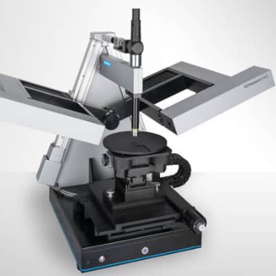
SENTECH SENresearch 4.0