Company type
Home | Mitglieder |
Fraunhofer-Institut für Zuverlässigkeit und Mikrointegration – IZM ASSID
Research institution
Target markets
Electronics·Energy·Food·Infrastructure·Life science·Mobility·Water and Environment
Industries
Research & Development
Portfolio
3D Wafer-Level-Packaging·Customer-specific prototyping·Electronic·Heterogeneous 3D Integration·Medical Technology / Pharma·Micro- / Nanoelektronics·Research Institutes·Semiconductor Industry·Smart Systems
Certificates
Contact
Ringstraße 12
01468 Moritzburg
01468 Moritzburg
+49/351/795572-0
Contact Person
Dr. Manuela Junghähnel
Head of Fraunhofer IZM ASSID
About this member
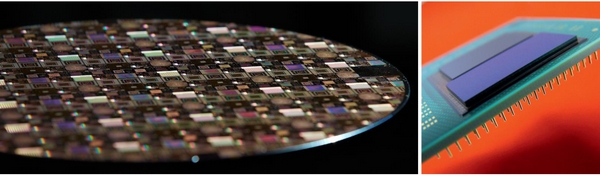
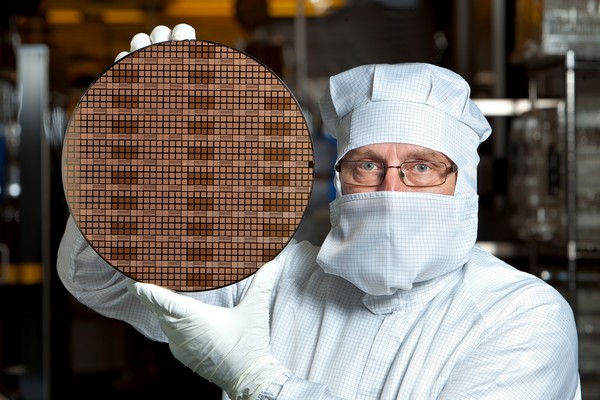
Fraunhofer IZMs Center “All Silicon System Integration Center Dresden – ASSID” was established in 2010 and is integral part of Fraunhofer IZMs wafer level system packaging and system integration. IZM-ASSID operates a state-of-the-art 300mm process line for 3D wafer level system integration based on Cu-Through Silicon Via technology. Constituent parts of the line are individual process modules for TSV formation, TSV post-processing as well as assembly and 3D stacking. The process line allows an application oriented development of 3D wafer level processes as well as the qualification and prototype manufacturing for 3D wafer level system in packages. Typical application fields are High Performance & Quantum Computing, Edge Sensor Systems, e.g.
3D stacking/ bumping
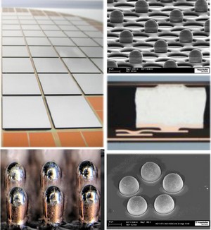
3D-Assembly and Interconnection Technologies
- Evaluation of die-to-wafer (D2W) and wafer-to-wafer (W2W) bonding for 3D stack formation
- 3D IC assembly with high-density interconnects (> 1000 I/O) and ultra-fine pitch (< 50 μm)
- 3D IC assembly with thin and ultra thin Chips (20 –150 μm)
Heterogeneous 3D system integration, 300mm
Fraunhofer IZMs center »All Silicon System Integration Center Dresden« (ASSID) was established in 2010 and is integral part of Fraunhofer IZMs wafer level system packaging and system integration. Fraunhofer IZM-ASSID operates a state-of-the-art 300 mm process line for 3D wafer level system integration based on Cu-Through Silicon Via (Cu-TSV) technology. Constituent parts of the line are individual process modules for TSV formation, for TVS post-processing as well as assembly and 3D stacking. The process line allows an application oriented development of 3D wafer level processes as well as the qualification and prototype manufacturing for 3D wafer level System in Packages, CSP, and others. Fraunhofer IZM-ASSID is a member of Silicon Saxony e. V. and is closely cooperating with customer, equipment and material supplier as well as with several organizations, networks and cluster (e.g. EMC-3D, ITRS, Sematech), especially in the field of 3D integration. Furthermore there exist close cooperation with Fraunhofer institutes and other scientific-technical institutions in the Free State of Saxony.
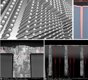
TSV Formation
Through Silicon Via (TSV) Formation
- High-density TSV technology for advanced system performance
- Via-middle/Via-last process integration
- Cu-TSV filling using high-speed ECD
- TSV post processing on wafer front and back side
- Evaluation and validation of new materials for TSV filling and isolation
- High yield TSV process integration
TSV interposer
TSV Interposer with high-density Multi-Layer Metallization
- Silicon Interposer with high-density Cu-TSV
- Both sided high-density multi-layer Cu-wiring
- Integration of active and passive devices
- Compatible interconnects for 3D stacking of silicon components for wafer level assembly (D2W, W2W) and package/board-assembly