Company type
Home | Mitglieder |
Eurofins MASER B.V.
Medium-sized companies (<250 employees or <50 million annual turnover)
Target markets
Electronics·Life science·Machinery and Equipment·Services
Industries
Materials·Research & Development·Technology
Portfolio
Advanced Packaging·Aerospace·Biotechnology·Computers·Electronic·Energy Systems·Environmental Technoloy·Equipment·Material analysis·Medical Technology / Pharma·Micro- / Nanoelektronics·Photovoltaics·qualification·Rail / Automotive·Semiconductor Industry
Certificates
Contact
Auke Vleerstraat 26
7521 PG Enschede
7521 PG Enschede
+31534802687
Contact Person
Thijs Kempers
+31657591958
CEO
About this member
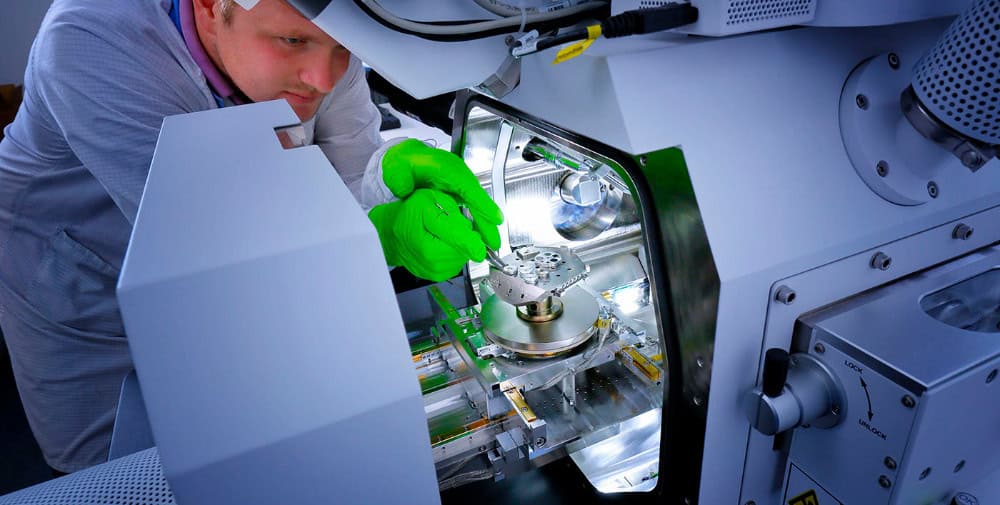
Eurofins MASER is an independent engineering service company. Since 1993 we have offered Reliability Test and Failure Analysis Services to the semiconductor and electronic systems industry.
Whether your company is active as Fabless Semiconductor Manufacturer, IC Design House, Electronic Manufacturing Service (EMS) Provider or Original Equipment Manufacturer (OEM) we can support you with your daily Reliability Test or Failure Analysis challenges.
We look forward to supporting you!
Whether your company is active as Fabless Semiconductor Manufacturer, IC Design House, Electronic Manufacturing Service (EMS) Provider or Original Equipment Manufacturer (OEM) we can support you with your daily Reliability Test or Failure Analysis challenges.
We look forward to supporting you!
Failure analysis service
NON-DESTRUCTIVE ANALYSIS
• High magnification optical microscopy
• DC parametric test (IV curve tracing)
• High resolution 2D X-ray microscopy
• CT X-ray microscopy (3D X-ray)
• Scanning Acoustic Microscopy (SAM)
• (3D) Non-destructive Lock-In Thermography inspection (LIT)
SAMPLE PREPARATION
• Laser ablation decapsulation
• Wet chemical decapsulation / etching
• Microwave Induced Plasma decapsulation (MIP)
• Mechanical grinding/polishing/decapsulation
• Front and back side delayering
• Automated selected area polishing (ASAP micro polishing)
• Dual-Beam cross-sectioning / TEM sample preparation
FAILURE LOCALIZATION
• Photon Emission Microscopy (PEM / EMMI)
• Optical Beam Induced Resistance Change (OBIRCH)
• (3D) Lock-In Thermography (LIT)
• Conductive Atomic Force Microscopy (C-AFM)
• Passive Voltage Contrast inspection (PVC)
IMAGING
• Low power stereo microscopy
• Bright Field / Dark Field high power optical microscopy
• Through silicon Back Side NIR Laser Patterning (BSLP)
• High resolution Scanning Electron Microscopy (SEM)
• Focused Ion Beam imaging (FIB)
• (Scanning) Transmission Electron Microscopy ((S)TEM)
Failure Analysis service