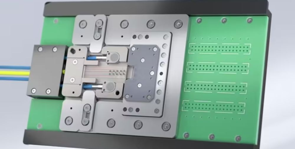
Time-saving parallel testing at high cycle rates
The consistent further development of the patented technology expands the possibilities of optical coupling and, with the new UFO Probe® Vertical version, enables parallel functional testing of optical as well as electrical components on chips using vertical needle technology from established probe card manufacturers. This allows users to couple up to 32 – or more if required – optical channels in parallel as standard, without the need for active alignment.
Thanks to this advantage and the time-saving parallel testing of optical and electrical components on wafers, the UFO Probe® Vertical is particularly suitable for use in high-volume production. There, functional tests at wafer level are an important cost factor. With the help of the UFO Probe®, information about the functionality of the individual chips is available even before the subsequent process steps, such as dicing and packaging. Defective chips can thus be removed from the further process at an early stage. This increases yield and reduces follow-up costs.
The UFO Probe® Vertical serves the entire wavelength range from 1260 to 1625 nanometers used in the telecommunications and data communications sector. Another new feature is the option of providing polarization preservation for individual or all optical channels.
Powerful test solution for increased requirements
By combining it with vertical-needle technology, Jenoptik is serving the increased market requirements, particularly with regard to so-called co-packaged optics. Here, a trend towards smaller chips with significantly more and thus smaller as well as more densely packed electrical contacts can be observed. With the UFO Probe® Vertical, up to 6,000 bond pads with dimensions of up to a minimum of 35 micrometers can be contacted, or even more depending on the needle type. Even solder bumps or copper pillars are no problem. The smallest addressable pitch of the electrical contacts is in the range of 40 to 80 micrometers. Furthermore, the vertical needles allow a smaller and more uniform contact resistance in the range of 0.2 to 1.0 Ohm depending on the needle type, while minimizing probe marks. These advancements ensure economical use in high-volume test scenarios and ATE connections.
Jenoptik will showcase the UFO Probe® at the ECOC trade show in Glasgow, Scotland, October 2-4, 2023, booth 736.
Images are available in the Jenoptik image database under “Products”.
About Jenoptik
Optical technologies are the basis of our business: Jenoptik is a globally operating photonics group and active in the two divisions Advanced Photonic Solutions and Smart Mobility Solutions. Our key markets primarily include Semiconductors & Electronics, Life Science & Medical Technology, and Smart Mobility. In fiscal year 2022, Jenoptik generated sales of 980.7 million euros.
The Jenoptik Advanced Photonic Solutions division is a global OEM and machinery supplier for photonics-based solutions. Our expertise spans a broad portfolio of technologies in optics, laser technology, digital imaging, optoelectronics, sensor technology, and optical test and measurement solutions. As an “enabler”, we serve leading machine and system builders in semiconductor manufacturing, laser material processing, life science and biophotonics, industrial automation, automotive and security industries. As a reliable and flexible development and production partner, we apply our expertise in key technologies to solve our customers’ most demanding requirements. With our systems, modules and components, we enable our customers to master their challenges with photonics.
– – – –
Further links
👉 www.jenoptik.de
Photo: Jenoptik