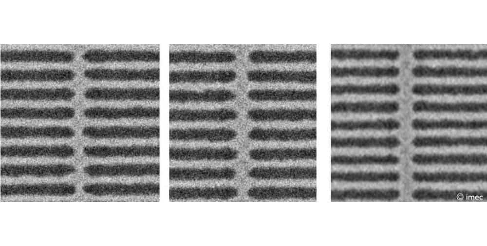
After demonstrating 20 nm pitch metallized line structures at SPIE Advanced Lithography and Patterning 2025 in February 2025, imec now achieves 20 nm pitch line structures with a critical dimension (CD) of 13 nm from tip to tip (T2T) with a single exposure step of high-NA EUV lithography. A local CD uniformity (LCDU) of only 3 nm was measured for the 13 nm T2T structures, which represents a milestone in the industry. The results were achieved with a metal oxide resist (MOR) that was optimized along with the underlayer, illumination pupil shape and mask selection.
Steven Scheer, Senior Vice President Compute System Scaling at imec: “Realizing these logic designs with a single high-NA EUV lithography reduces processing steps compared to multi-patterning, lowers manufacturing costs and environmental impact, and improves yields. These results support Damascene metallization, the industry standard for compound manufacturing. T2T structures are an essential part of the interconnect layers as they enable disruption of the one-dimensional metal tracks. To meet the logic roadmap at a metal pitch of 20 nm, the T2T pitch is expected to be scaled to 13 nm and below while maintaining functional interconnects. Developments are underway to further scale the T2T dimensions, with promising results for 11 nm T2T, and to transfer the structures into an underlying hard mask – enabling true (double) Damascene interconnects.”
To enable metallization below 20 nm, the industry will likely move to alternative metallization processes. As a second achievement, imec demonstrates the compatibility of direct metal etching (DME) of ruthenium (Ru) with single exposure high NA-EUV lithography. We have realized 20 nm and 18 nm Ru lines, including 15 nm T2T structures and low resistance functional interconnects. An electrical test yield of 100% was achieved for the metallized line structures with 20 nm pitch.
Steven Scheer: “Following the opening of the joint ASML-imec High-NA-EUV lab in Veldhoven, the Netherlands, imec and its partner ecosystem have made great progress in advancing High-NA-EUV lithography and bringing the industry into the Angstrom era – supported by three years of ecosystem preparation. The results presented mark a new milestone and underline imec’s leadership in lithography research and development. They also play a crucial role in realizing the goals of the European Chips Act to enable logic technology nodes below 2 nm. Working closely with the imec-ASML High NA EUV ecosystem, which includes leading chipmakers, equipment, material and resist suppliers, mask manufacturers and metrology experts, we continue to jointly optimize High NA EUV lithography and patterning in support of logic and memory roadmaps.”
About imec
Imec is a world-leading research and innovation center for nanoelectronics and digital technologies. Imec leverages its state-of-the-art R&D infrastructure and its team of more than 6,000 employees and top researchers for research and development in advanced semiconductor and system scaling, silicon photonics, artificial intelligence, 5G communications and sensor technologies, as well as in application areas such as health and life sciences, mobility, industry 4.0, agri-food, smart cities, sustainable energy, education, etc. Imec brings together global leaders in the semiconductor value chain, Flanders-based and international technology, pharmaceutical, medical and ICT companies, start-ups, universities and knowledge centers. Imec is headquartered in Leuven (Belgium) and has research sites in Belgium, the Netherlands, the UK and the US as well as offices on three continents. In 2024, imec’s turnover (P&L) amounted to a total of 1.034 billion euros.
– – – – – –
Further links
👉 www.imec-int.com
Photo: imec