Applied Materials, Inc. and the Fraunhofer Institute for Photonic Microsystems IPMS, Germany’s leading research center for semiconductors at 300 mm, today announced a landmark collaboration to establish one of the largest technology centers for semiconductor metrology and process analysis in Europe.
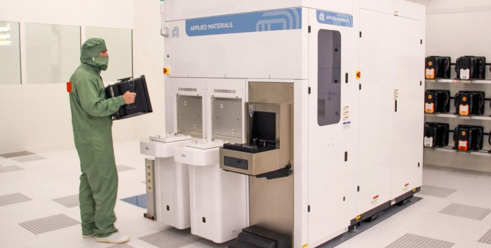
The technology center, which will be located at the Center Nanoelectronic Technologies (CNT) of Fraunhofer IPMS in Dresden, is situated in the heart of Silicon Saxony, the largest semiconductor cluster in Europe. The technology hub will be equipped with state-of-the-art eBeam metrology equipment from Applied Materials, including the VeritySEM® CD-SEM system (a critical-dimension scanning electron microscope), and will be supported by Applied Materials engineers and R&D experts.
“Fraunhofer IPMS and its partners will benefit from access to Applied’s industry-leading eBeam metrology systems,” said Dr. Benjamin Uhlig-Lilienthal, head of the Next Generation Computing business unit at Fraunhofer IPMS. “The new technology hub will enable advanced wafer-level metrology in our industrial CMOS environment with the unique capability of Fraunhofer IPMS to exchange wafers directly with semiconductor manufacturers.”
“Our joint metrology hub will accelerate learning cycles and the development of new applications for the Fraunhofer Institute, Applied Materials and our customers and partners in Europe,” said James Robson, corporate vice president for Applied Materials Europe. “This unique center of excellence will be able to test and qualify processes on a wide range of substrate materials and wafer thicknesses that are critical for applications in Europe’s diverse semiconductor landscape.”
Measurement technology is critical in microchip manufacturing, providing precise measurements needed to accurately monitor and control the quality of each step and process in semiconductor manufacturing. Chip manufacturers use measurement equipment at critical points to validate physical and electrical properties and ensure target yields.
About Applied Materials
Applied Materials, Inc. (Nasdaq: AMAT) is the leading provider of solutions for the semiconductor technologies that make virtually every new chip and advanced display in the world. Our expertise in modifying materials at the atomic level and at industrial scale enables our customers to turn the latest developments in the semiconductor process into reality and scale. Applied Materials makes a better future possible with its innovations.
About Fraunhofer IPMS
The Fraunhofer Institute for Photonic Microsystems IPMS is a leader in applied research and development in the fields of smart industrial solutions, medical technology and mobility. Fraunhofer IPMS works on electronic, mechanical and optical components and their integration into miniaturized devices and systems. Its services range from conceptual design and product development to pilot production in its own laboratories and clean rooms. With the Center Nanoelectronic Technologies (CNT), Fraunhofer IPMS offers applied research on 300 mm wafers for microchip producers, suppliers, device manufacturers and R & D partners.
*ICAPS = Internet of things, Communications, Automotive, Power and Sensors
Contact
Dr. Benjamin Lilienthal-Uhlig
Next Generation Computing (NGC)
Fraunhofer IPMS (Center Nanoelectronic Technologies CNT)
An der Bartlake 5
01109 Dresden, Germany
Telephone +49 351 26 07-3064
_ _ _ _
Further Links
👉 www.ipms.fraunhofer.de
Photo: Fraunhofer IPMS