Wafers are thin, circular slices of semiconductor material that serve as the basis for the production of microchips and other electronic components. The quality and purity of the wafer surface are crucial for the functionality and performance of the end products. Various characterization methods are used to detect and quantify contamination. These have now been expanded at Fraunhofer IPMS to include ultra-trace element analysis. After etching 200 or 300 mm wafers with HF vapor (hydrofluoric acid), a drop is applied to the wafer surface and moved over it. The drop collects the soluble residues present on the surface and is then filled to a volume of 1 ml. The dissolved elements are then analyzed using inductively coupled plasma mass spectrometry (ICP-MS). This method provides precise quantitative information about the dissolved elements on the wafer surface.
The ultra-trace element analysis offers extensive possibilities: For example, surface and bevel scans are performed to analyze 39 elements with RF scanning solution, which enables detailed characterization of the wafer surface. For special applications, aqua regia can also be used as a scanning solution for five precious metals.
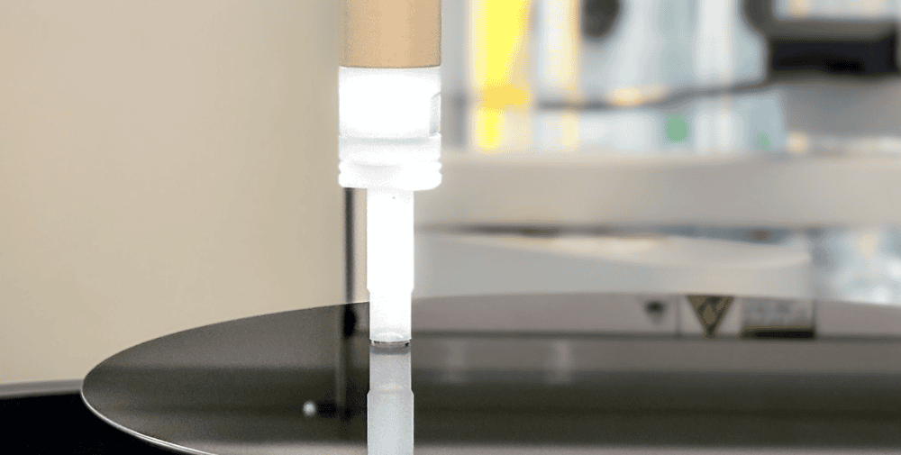
Laboratory equipment at Fraunhofer IPMS
The laboratory is equipped with state-of-the-art equipment, including the VPD system Wafer Surface Preparation System WSPS2 from PVA Tepla and the iCap RQ mass spectrometer from Thermo Scientific. These technologies enable accurate characterization and quality assurance in the semiconductor industry.
With this expansion, Fraunhofer IPMS consolidates its position as a leading research institute in the field of 300 mm wafer processing and contributes to the improvement of production quality in semiconductor manufacturing.
On the institute’s website, interested parties can find more information on the available characterization methods. You can also meet us at Analytica 2026 at the Fraunhofer booth A3 – #312.
About Fraunhofer IPMS
Fraunhofer IPMS is a leading international research and development service provider for electronic and photonic microsystems in the application fields of intelligent industrial solutions, medical technology and health, mobility as well as green and sustainable microelectronics. Research focuses on customer-specific miniaturized sensors and actuators, MEMS systems, microdisplays and integrated circuits as well as wireless and wired data communication. The services offered range from consulting and design to process development and pilot series production.
With the Center Nanoelectronic Technologies (CNT), Fraunhofer IPMS offers applied research on 300 mm wafers for microchip producers, suppliers, device manufacturers and R & D partners.
– – – – – –
Further links
👉 www.ipms.fraunhofer.de
Photo: Fraunhofer IPMS