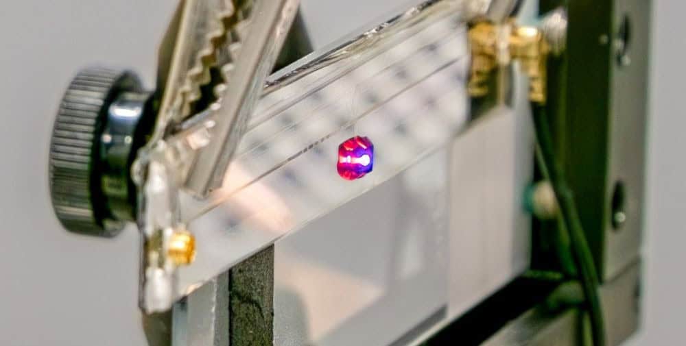
The principle of quantum sensing is based on NV diamonds (nitrogen-vacancy diamonds), which have unique properties due to defects in their crystal structure. NV centers can be optically excited and emit light whose photoluminescence is used to detect magnetic fields, electric fields or temperatures.
Patrick Engelmann, project manager at Fraunhofer IPMS, emphasizes the advantages of the new approach: “The newly developed CMOS-based platform for quantum sensing can easily be operated at room temperature due to the NV technology, where otherwise complex cryogenics is required. By integrating the light source, detector, microwave and readout on one chip, the system is highly miniaturized and consumes very little energy. In addition, we can achieve a spatial resolution in the micrometer range by using multi-channel arrays instead of individual measuring points. The system is robust and portable, as it does not require lasers or optics.”
The development of these CMOS-integrated quantum sensors opens up new horizons in various fields, from geophysics for exploring geomagnetic field deformations to medicine for heart and nerve monitoring and, in perspective, as an interface for brain-machine interaction. This technology addresses challenges that could not be solved so far, such as portable magnetic field quantum sensors for fast, highly sensitive on-site analysis and simplified laboratory workflows.
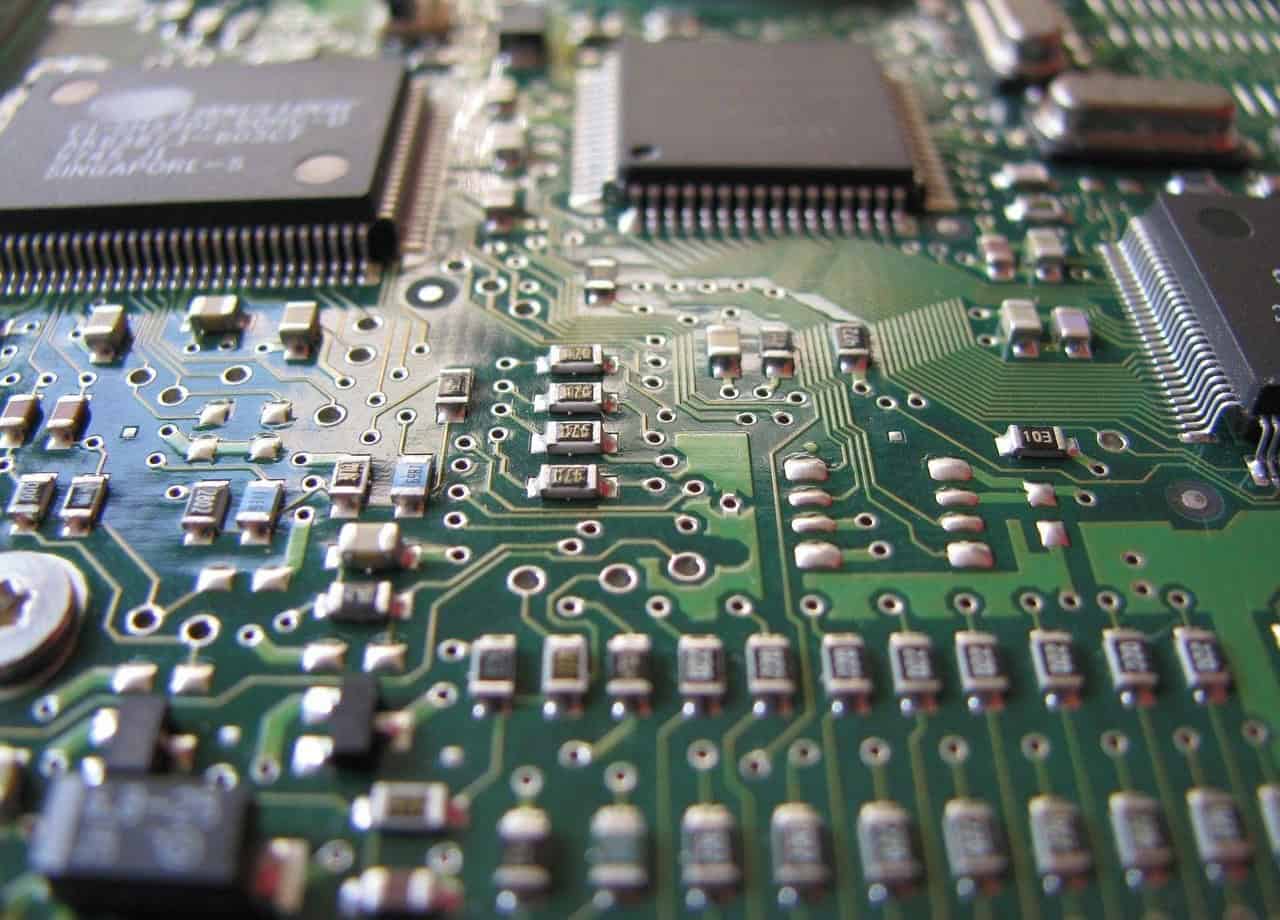
The required CMOS backplane is designed at Fraunhofer IPMS and manufactured in a commercial semiconductor factory. OLED light sources are then integrated onto the chip at the institute. The precise alignment of the NV diamonds to the sensor pixels is crucial for optimal measurement results. The work builds on the expertise available at the institute for the integration and production of OLED-on-silicon components. Specifically, they are based on the so-called “bi-directional” microdisplays with image recording and playback function on a chip.
In the joint project, the MPI CPfS is working on the measurement methodology, as well as the quantum optical material in the form of NV diamonds and alternative materials for this application.
So far, the joint integration of OLED and antenna as well as the excitation of the NV center has been demonstrated in a technology demonstrator. Work is still ongoing on the complete CMOS integration of the sensor system, including photodetectors and the complete readout circuit. Industrial partners have already expressed interest. Verification in initial research applications is expected in three to four years. If validation is positive, the platform can be quickly adapted to specific applications and transferred to pilot production.
– – – – –
Further links
👉 www.ipms.fraunhofer.de
Photo: Fraunhofer IPMS