During semiconductor production, up to 1500 process steps are carried out, including etching, deposition and lithography. Accordingly, there is a high potential for defects, although finished wafers should be virtually defect-free due to their highly complex structures. In order to guarantee these high quality standards, sometimes almost 50% of the process steps are accounted for by accompanying metrology processes and several thousand additional control wafers are often required per month. This approach therefore requires a considerable amount of additional work and therefore more financial and material resources as well as additional energy and time.
The “NEST” project (New Screening Tool for Efficient Semiconductor Production) has addressed precisely this problem: Within an environmental potential analysis conducted by DIVE, Fraunhofer IPMS and Fraunhofer IZM over the last 1.5 years, it was determined that targeted inspection tools can not only save at least 25% of inspection wafers, but also more than 118,000 kilograms of CO2 emissions per month during production. DIVE uses innovative spectroscopy and imaging technology that makes it possible to identify defects in deeper layers. The calculations were based on the conditions of a 28 nm production process and 25,000 wafer starts per month. The project was funded as part of the “Green ICT Space” of the Research Fab Microelectronics Germany (FMD).
In addition to the general reduction in emissions, the use of such screening tools offers further ecological benefits such as the saving of water and chemicals used in the production of control wafers. There is also an economic advantage if a large proportion of additional metrology steps can be saved. This is because the general energy balance is also improved by the reduced tool occupancy that would otherwise be caused by control wafers. Process deviations can be detected at an early stage, production errors are avoided and the productive wafer yield is positively influenced.
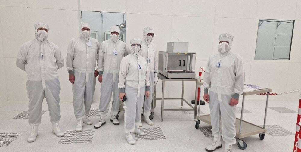
Industry-oriented evaluation in the Fraunhofer IPMS clean room
DIVE imaging systems GmbH develops innovative inspection tools that combine the advantages of optical spectroscopy with imaging. The DIVE VEpioneer® system is the first system from DIVE to operate under cleanroom conditions. The system detects surface properties, contaminants and deviations from production specifications within 20 seconds. Thanks to this rapid inspection and the additional use of AI algorithms, the process steps in semiconductor production can be comprehensively controlled and the testing effort is reduced. “DIVE’s hyperspectral imaging systems offer a new possibility for non-destructive testing of entire wafers. With the support of Fraunhofer IPMS, this innovative technology is now available for use in standardized industrial cleanrooms – enabling significant productivity increases and cost reductions for semiconductor factories,” says Martin Landgraf, R&D Manager at Fraunhofer IPMS.
Even after the successful completion of the project, the DIVE VEpioneer® system will remain at the Center Nanoelectronic Technologies (CNT) of Fraunhofer IPMS, where it will carry out further wafer measurements and evaluations for customers and partners. In further joint projects, the system is also to be further developed in the future with automation of wafer handling and equipment coupling for automatic data transfer. The takeover of DIVE imaging systems GmbH by PVA TePla AG opens up further evaluation and development opportunities for the start-up, particularly thanks to the expertise and experience of the materials and measurement technology specialist.
Contact
Martin Landgraf
Fraunhofer IPMS – Center Nanoelectronic Technologies CNT
An der Bartlake 5
01199 Dresden
Telephone +49 351 26 07-3004
Further links
👉 Fraunhofer IPMS website
Photo: Fraunhofer IPMS