By integrating Fraunhofer IPMS’ cutting-edge metrological expertise in advanced defect and contamination control, the partnership aims to improve and increase water recycling methods, reduce chemical consumption and optimize overall process efficiency – paving the way for smarter solutions in a water-scarce future.
Nano-pure water for sustainable water consumption
Industry analysis shows that water consumption in the semiconductor sector has increased by 20-30% in recent years, with the average chip manufacturing plant using up to 37 million liters (10 million US gallons) of UPW per day – an amount equivalent to the daily water needs of a city of 300,000 people. The production of ultrapure water has traditionally been associated with considerable costs. Due to the energy-intensive and chemical processes required, it can be 60 to 350 times more expensive than drinking water. This is the challenge that NSS Water is addressing with its nano-pure water (NPW). Water consumption in the semiconductor industry will continue to rise as more and more modern equipment with higher consumption will be needed in the coming years. Furthermore, 40% of chip production facilities are expected to be located in high water risk areas by 2030. This means that the need for data-driven, circular water strategies has never been greater.
“Water is the lifeblood of our planet and the backbone of the semiconductor industry,” says Reza Jafari Jam, Research Director at AlixLabs. “This joint research on water conservation not only protects a finite resource, but also supports innovation and ensures sustainable growth and technological progress. We are driving the semiconductor industry towards greater sustainability with our APS™ patterning process technology and our collaboration with NSS Water will further cement our position as a pioneer for the green semiconductor manufacturing of tomorrow.”
Collaboration for advanced semiconductor manufacturing
“We are excited to expand our collaboration with AlixLabs and Fraunhofer IPMS,” says Björn Holmström, CEO of NSS Water. “Advanced metrology will help us provide a platform that enhances the water infrastructure used by AlixLabs and other advanced semiconductor companies. This project will allow us to test our NPW on 300-millimeter wafers and have the wafers cleaned with NPW from Fraunhofer IPMS,” he adds.
Through this partnership, AlixLabs and NSS Water are combining their respective strengths in innovative water treatment, advanced analytics and semiconductor manufacturing expertise to develop solutions that significantly reduce water consumption, lower operating costs and promote sustainability.
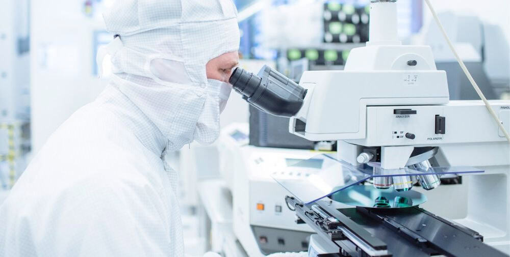
The support of Fraunhofer IPMS ensures precise control of impurities and defects, further increasing the effectiveness of the recycling and purification processes. The project is co-funded by the European nanoelectronics access program ASCENT+, which provides direct access to Europe’s global nanoelectronics research infrastructure and enables researchers, SMEs and PhD students to access state-of-the-art capabilities. The project is an important step in positioning AlixLabs, NSS Water and the European Union at the forefront of sustainable innovation in semiconductor manufacturing.
– – – – –
Further links
👉 www.ipms.fraunhofer.de
Photo: Fraunhofer IPMS