

“Chiplets will play an important role for the global semiconductor industry in the coming years. This is because this technology offers the greatest degree of freedom in the customized design of electronic systems. It is therefore all the more important that the European economy has a coordinated roadmap for the development of its own products and the use of chiplets.” Andy Heinig, Head of Department at Fraunhofer IIS/EAS and Head of the Chiplet Center of Excellence (CCoE), is convinced of this. “It is therefore essential for companies to be able to assess the feasibility of system solutions based on chiplets at an early stage. To this end, we at the CCoE keep an eye on the broad spectrum of requirements and boundary conditions for the products and use them to develop practical workflows and new methods for evaluation.”
The CCoE aims to support the competitiveness and technological sovereignty of strong European industrial sectors. In the first two years, the center will therefore focus on applications in automotive electronics. To this end, various key partners along the value chain will be brought together – from car manufacturers to semiconductor producers. The Fraunhofer researchers want to develop methodological approaches, architectural concepts, reusable basic components and roadmaps for the development, production and robust design of chiplets for them. In addition, they will evaluate various chiplet solutions at the center in terms of their performance, costs and reliability. Research results will also be incorporated into international standardization and contribute to the design of a cross-manufacturer chiplet ecosystem.
The unique position of the CCoE results from the broad Fraunhofer portfolio in electronics development and production as well as the close, interdisciplinary cooperation with industry. The Center is managed by the Dresden branch of the Fraunhofer Institute for Integrated Circuits IIS, the Fraunhofer Institute for Reliability and Microintegration IZM and its All Silicon System Integration Dresden – ASSID branch, as well as the Fraunhofer Institute for Electronic Nano Systems ENAS. Interested companies that want to participate in the CCoE’s pre-competitive work and help shape its research agenda can join the center until autumn 2024. Further information on the CCoE and contact details can be found on the following website: www.chiplet-center.fraunhofer.de.
Background: Chiplets
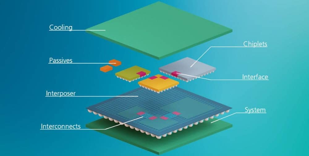
Electronics solutions based on chiplets make it possible for the first time to integrate different functional units, even in different technologies, on a single substrate or in a 3D chip structure. This gives electronics developers the opportunity to use the most suitable production technologies. For example, the latest and most expensive technologies for certain functionalities can be concentrated on a few circuits instead of having to use them for the entire chip structure. Today, the use of chiplets is already economical for mass-produced applications and is being introduced primarily by US companies in the data center sector. However, proprietary standards are used for this. Implementation with chiplets from various sources for product groups in small and medium quantities, such as for automotive applications, has so far been largely excluded from this.
About Fraunhofer IIS/EAS
The Fraunhofer Institute for Integrated Circuits IIS stands for cutting-edge international research into microelectronic and information technology system solutions. The scientists at the EAS branch in Dresden are working on new design concepts to counter the constant miniaturization of semiconductor components and the growing complexity of integrated circuits. The branch also contributes this expertise to the work at the CCoE. For example, application-specific design processes, new packaging concepts for chiplet solutions, test structures or adapted interface IP are developed. The overall management of the Chiplet Center of Excellence is also based here.
About Fraunhofer IZM
For over 30 years, Fraunhofer IZM has been one of the world’s leading institutions for applied research and development of robust and reliable electronics and their system integration at wafer, chip and board level. Over 450 employees find technological solutions for future challenges such as high-end performance packaging, quantum sensor technology, hardware security and bioelectronics, sustainable 6G applications or chiplets. At the Chiplet Center of Excellence, Fraunhofer IZM will be responsible for the realization of demonstrators and in particular contribute its expertise in wafer-level assemblies and substrates. Process lines for 200 and 300 mm 3D wafer level processes and a 600 mm substrate line are available for this purpose.
About Fraunhofer ENAS
Fraunhofer ENAS is a research and development partner in the field of intelligent systems for a wide range of applications. The Chemnitz-based institute contributes its many years of expertise in testing, reliability assessment and the characterization of solutions in the field of electronics and smart systems integration to the CCoE. Fraunhofer ENAS will develop methods for the virtual testing and prototyping of chiplet components and systems, with which the functionality and reliability of chiplet solutions can be optimized in a significantly more time and resource-efficient manner.
– – – – – –
Further links
👉 www.eas.iis.fraunhofer.de
Photo: Fraunhofer IIS/EAS


