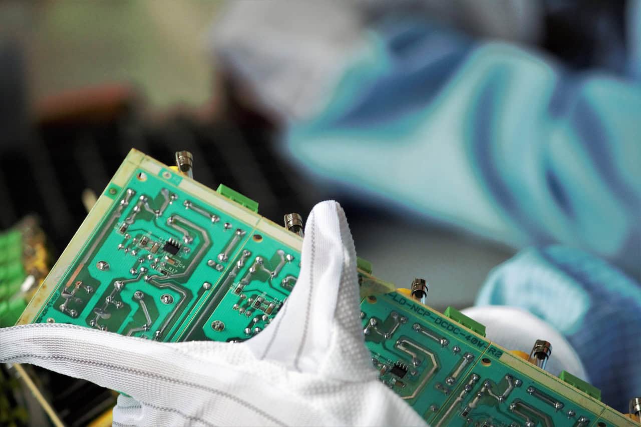
The aim of the collaboration is to develop a new type of etching process for the micro- and nanotechnological processing of silicon, which is crucial for the manufacture of semiconductor components. To this end, the three partners are relying on a high-performance etching process for semiconductors in the form of metal-assisted chemical vapor etching (so-called “gas-phase metal-assisted chemical etching” or “gas-MacEtch” technology). This process can be used to produce micro- and nanostructures with extremely high aspect ratios and particularly straight, smooth sidewalls in a controlled, reproducible and high-quality manner. It combines unsurpassed structural precision and design freedom with extreme speed and is also ideal for large-area processing and structuring of wafer surfaces.
The “Gas-MacEtch” technology is based on a catalytic reaction between a metal catalyst, which is applied to the surface of the silicon substrate to be etched, and a gaseous etching chemical. Contact with the etching chemistry leads locally to an accelerated chemical reaction in which the catalyst material penetrates vertically into the silicon substrate and leads to the formation of finely etched functional structures with precise geometries.
Ecologically and economically sustainable: New era of chip production with resource-saving etching process
“The new process completely eliminates the use of PFAS compounds. The alternative use of environmentally friendly and biodegradable chemicals and gases significantly reduces harmful environmental impacts during wafer structuring and makes an active contribution to greater sustainability in semiconductor manufacturing,” explains Micha Haase, head of the “Plasma Etching and Process Diagnostics” group at Fraunhofer ENAS, who is developing the new process together with partners from the Paul Scherrer Institute PSI and memsstar Limited.
These advantages of the “Gas-MacEtch” process are complemented by another environmentally friendly aspect: compared to established etching processes, the etching process enables silicon wafers to be structured at significantly lower temperatures. This improves the energy balance of semiconductor production, reduces greenhouse gas emissions and significantly lowers energy costs.
Worldwide: Necessary switch to PFAS-free products and processes
The growing complexity of legal requirements from the EU and global regulatory bodies to reduce PFAS in response to global health and environmental concerns is increasing the pressure on the industry in the long term and demanding a change of direction. For the semiconductor industry, this means not only new challenges in complying with applicable environmental regulations and requirements, but also an active responsibility in the development of sustainable production technologies and environmentally friendly PFAS alternatives.
“Our research into a PFAS-free etching process for the chip industry takes precisely these international dynamics and developments into account. The combination of environmental protection and technological progress represents a decisive competitive advantage for chip manufacturers that meets new legal requirements, positions the European semiconductor industry as an innovation leader in the global economy and ensures the long-term sustainability of the industry through the use of innovative technologies,” explains Micha Haase.
The work of the researchers ultimately has far-reaching positive effects for society and the environment, the scientist continues. The consistent avoidance of toxic substances in wafer processing makes an active contribution to minimizing risks to nature and health. “As PFAS is suspected of damaging entire ecosystems through its decades of use, accumulating in the human body via the food chain and causing cancer, turning away from toxic industrial chemicals and replacing them with harmless substances also underlines our awareness in science of our social responsibility,” explains the researcher.
Three countries, one goal: Strong European partners unleash potential for sustainable semiconductor manufacturing
Fraunhofer ENAS, the Paul Scherrer Institute PSI and memsstar Limited are working closely together to get closer to the goal of a PFAS-free future in semiconductor manufacturing:
As part of the collaboration, Fraunhofer ENAS in Chemnitz is developing and optimizing the “Gas-MacEtch” process and ensuring its seamless integration into industrial manufacturing environments. The Paul Scherrer Institute PSI in Villingen, Switzerland, with its proven expertise in the field of “Gas-MacEtch” technology, uses state-of-the-art analytical methods to investigate and optimize the catalytic reaction partners and the chemical interaction between different material systems that takes place during the etching process. As Europe’s leading process and equipment supplier of etching and deposition solutions for semiconductor and MEMS manufacturing processes, memsstar Limited from Livingston in the UK provides a cluster tool for vapor phase etching of silicon oxide and silicon deep etching using “Gas-MacEtch” technology with its “Orbis-3000” platform and is driving forward the technical implementation and scaling of the process in industrial-scale systems. In this way, scientific depth, process know-how and industrial implementation power are combined to realize the new etching process efficiently and sustainably and to transfer it into application.
Innovation in use: fields of application with prospects
As a key technology for the next generation of semiconductor components, the new etching process can be used in the future for the production of 3D NAND memory, for example, a new development in flash memory chips in which memory cells are stacked vertically for a significant increase in storage capacity and speed.
The production of high-precision photonic crystals for optical applications is another example of the use of the “Gas-MacEtch” process. These structures require extremely smooth sidewalls and high aspect ratios in order to efficiently guide and manipulate light. Established processes have so far reached their limits in the production of such structures. The new etching process using “Gas-MacEtch” technology overcomes these hurdles, which were characterized by roughness or geometric limitations, and enables the precise and large-area production of photonic crystals or other photonic components. This opens up new applications in optical data transmission, sensor technology and quantum communication.
About memsstar Limited
Memsstar Limited is a leading provider of deposition and etching equipment, technology products and services for semiconductor and microelectronic mechanical systems (MEMS) manufacturers. The company’s etch and deposition equipment and technology solutions support the European semiconductor market and the global MEMS market. With its process technologies and equipment, memsstar Limited strengthens the MEMS industry in meeting the challenges arising from the development and manufacture of increasingly complex and integrated MEMS devices.
About the Paul Scherrer Institute PSI
The Paul Scherrer Institute PSI is the largest research institute for natural and engineering sciences in Switzerland and conducts cutting-edge research in the fields of future technologies, energy and climate, health innovations and the fundamentals of nature. At the Paul Scherrer Institute PSI, researchers are looking for previously unknown ways to process and store data, to make technologies more sustainable and efficient or to develop new processes in order to penetrate ever deeper into the micro and nano world. Their findings form the basis for new applications – be it in medicine, information technology, energy generation and storage – or for new production processes in industry.
– – – – – –
Further links
👉 www.enas.fraunhofer.de
Photo: pixabay