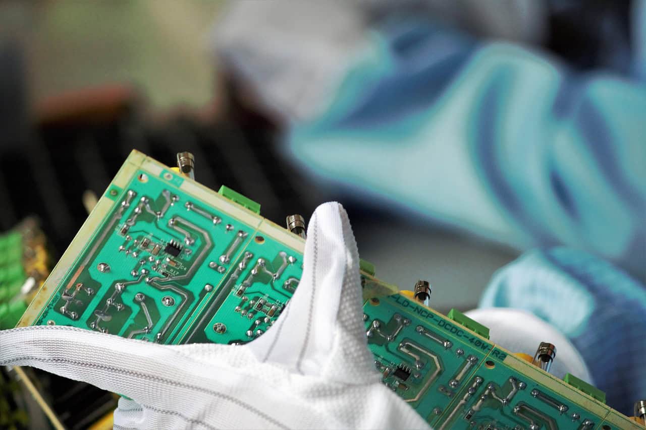
Chipmetrics, a leading provider of innovative measurement solutions for atomic layer deposition (ALD) and advanced semiconductor processes, announces the expansion of its test chip portfolio with the new ASD-1b area-selective deposition chip, a high surface area (HSA) wafer and pre-coated high aspect ratio (HAR) test structures, including PillarHall and VHAR1 test chips.
The new offerings – ASD-1b, the HSA wafer and the pre-coated high aspect ratio test structures – enable researchers and engineers to simulate real-world operating conditions with unprecedented precision, shortening development cycles and improving process optimization and control in advanced semiconductor manufacturing.
The new metrology tools at a glance
1. ASD-1b – Next Generation Area Selective Deposition (ASD) Test Chip
The newly launched ASD-1b chip builds on the original ASD-1 platform and offers the following features:
- High-resolution narrow lines with a unique three-color material layout, including a metal layer, ideal for testing self-aligned deposition processes.
- Material support for SiO₂, Si₃N₄ and metal surfaces.
- Compatibility with ALD, CVD and electroless plating techniques.
- Chip size of 15 × 15 mm with over 1,200 lines on a 6 × 6 mm area.
This advanced layout enables detailed evaluation of selectivity and defectivity on different surface materials and provides a faster way to validate ASD process schemes.
2. High Surface Area (HSA) Wafer – Increased Sensitivity for Material Studies
Thanks to Chipmetrics’ VHAR1 architecture, the new HSA wafer offers a significantly larger surface area due to deep trench structures:
- Trenches are etched up to 200 µm deep into a 150 mm VHAR1 wafer embedded in a 300 mm pocket wafer.
- The surface area is up to 300 times larger than flat wafers.
- The trenches can be adjusted in depth, making them ideal for sensitive film growth studies and material analysis.
This solution meets the growing need for highly sensitive metrology in thin film deposition and characterization environments and provides another option for rapid prototyping and process control.
3. Pre-coated VHAR1 and PillarHall® test structures
To better meet the needs of semiconductor companies and simulate realistic process conditions, Chipmetrics now also offers the following well-known products with improved coatings:
- Pre-coated HAR test chips with ALD films in the 10-50 nm range.
- Vertical (VHAR1, AR = 200) and lateral (PillarHall®, AR > 1000) geometries.
- Realistic film penetration and conformance profiles on actual coated substrates.
These pre-coated structures meet the growing demand for evaluating deposition uniformity and film conformity on application-specific substrates.
Accelerating process prototyping: available immediately
“With these new additions to our portfolio, we are enabling development teams to dramatically shorten feedback loops in thin film R&D,” said Mikko Utriainen, CEO of Chipmetrics. “Building on the proven capabilities of VHAR1, ASD-1 and our PillarHall test chips, we are giving engineers the tools they need to benchmark new chemistries and deposition processes more accurately and efficiently – bringing clarity and speed to process development and monitoring like never before.”
The new pre-coated HAR test structures, ASD-1b and HSA wafers, will be available to order from August 2025.
About Chipmetrics
Chipmetrics Oy develops and supplies metrology solutions for manufacturing processes in the semiconductor industry with a focus on innovative metrology chips and ALD measurement services. The main product is the PillarHall® metrology chip for near-instant conformance measurement of thin film processes. The company was founded in 2019 and is headquartered in Joensuu, Finland, with employees and sales partners in Japan, South Korea, the USA and Germany.
Translated by DeepL
– – – – – –
Further links
👉 https://chipmetrics.com
Photo: Chipmetrics