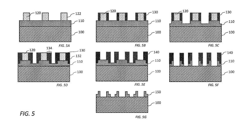
The new patent, internally referred to as the “Tetris” patent in honor of Alexey Pajitnov, integrates self-aligned double patterning (SADP) with atomic layer etch (ALE)-based pitch splitting technology (APS™). This innovative approach, which has been industrialized since AlixLabs was founded in 2019, combines elements of classical and state-of-the-art techniques to achieve superior performance for semiconductor manufacturing.
The invention grew out of AlixLabs’ efforts to develop a process to precisely control the sidewall angle in APS™, a key component in silicon-based processes. By utilizing the selectivity of the plasma etch process and combining features of complex plasma processes, AlixLabs has developed a method that combines the traditional SADP process with advanced APS technology.
This allows the company to leverage mature industry technologies while benefiting from the advanced control and improved performance of cyclic processes and topographic selectivity. As a result, AlixLabs’ solution provides semiconductor manufacturers with an improved ability to overcome the challenges of patterning at sub-5nm nodes.
This breakthrough is significant for the integration of APS™ technology into existing semiconductor manufacturing workflows by maintaining the use of existing process design kits (PDKs), which are essential tools for chip designers. This reduces barriers to the use of APS in high-volume manufacturing (HVM) and facilitates the transition to next-generation semiconductor technologies.
The patented innovation provides semiconductor manufacturers with greater flexibility and a new way to precisely tailor the APS™ process to customers’ advanced technology node requirements to reduce capital and operating expenses (CapEx and OpEx) and emissions, while enabling broader compatibility with different materials. This new method further strengthens AlixLabs’ core APS™ patent portfolio and positions the company as a leading enabler for next-generation semiconductor manufacturing.
In addition, this invention not only supports the development of cutting-edge logic, memory and photonics, but also simplifies the semiconductor manufacturing process by reducing CapEx and OpEx for semiconductor fabs.
“We remain committed to advancing semiconductor manufacturing with innovations that significantly improve the precision, flexibility and efficiency of our technologies,” commented Dmitry Suyatin, co-founder and CTO of AlixLabs. “This patent is an important step forward in our mission to drive the next generation of semiconductor processes and further solidify our position as a market leader in this space.”
– – – – –
Further links
👉 www.alixlabs.com
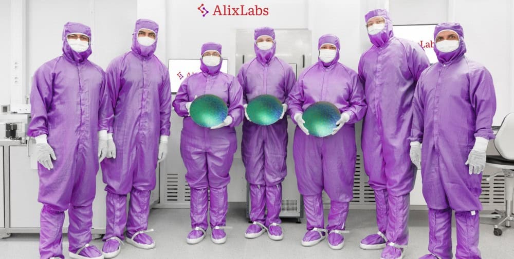
Photo: Alixlabs