Unternehmensart
Startseite | Mitglieder |
AlixLabs AB

Kleine Unternehmen (<50 Mitarbeiter:innen oder <10 Mio. Jahresumsatz)
Zielmärkte
Elektronik
Branchen
Produktion
Portfolio
Atomic Layer Etching·Halbleiterindustrie·Lithography·Mikro- / Nanoelektronik·Pattering·Prozess-Service
Zertifikate
Kontakt
Scheelevägen 15
22370 Lund
22370 Lund
+46 767639467
Ansprechpartner
Über das Mitglied
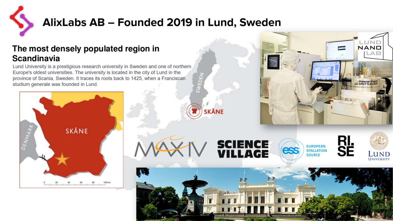
Currently, we are taking on the first round of private investments and will expand operations for both core activities in Lund, Sweden, at NanoLund and Lund Nano Lab, and the IDEON Science Park in Sweden.
After founding the company in 2019 we now move into very exciting times. The team has been expanded with Dr. Mohammad Karimi as Principal Scientist and we have several applications and projects in the pipeline for broadening our patent protection and creating further opportunities for commercial agreements starting now. Currently, we are taking on the first round of private investments and will expand operations for both core activities in Lund, Sweden, at NanoLund and Lund Nano Lab, and the IDEON Science Park in Sweden. In addition, we are heading to the heart of the European semiconductor industry in Dresden Germany for a lab to fab transfer to 300 mm silicon wafer process verification to get ready for customer demonstrations of APS.
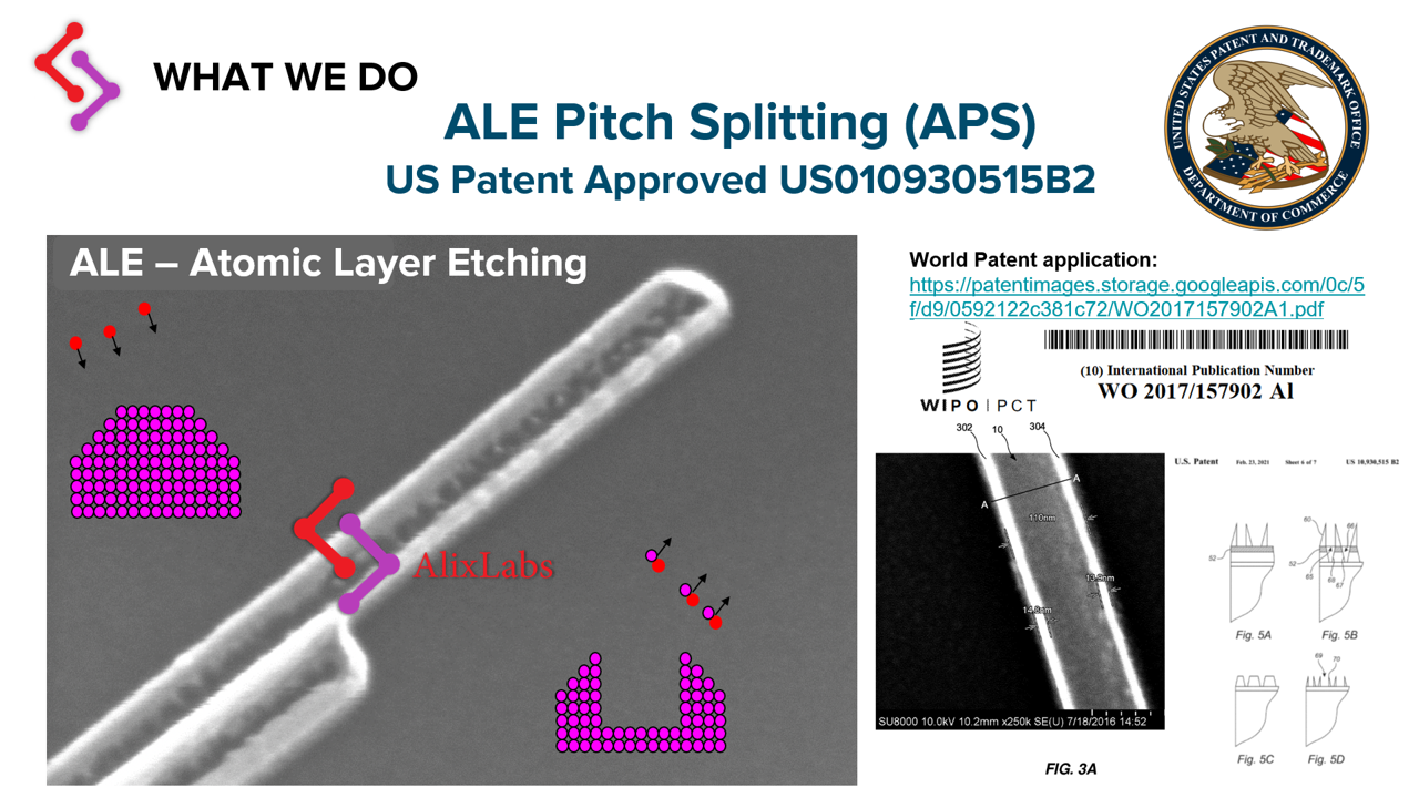
The US Patent Office has issued a patent (US10930515) on February 23, 2021. The patent covers methods to split nanostructures in half by a single process step using Atomic Layer Etching (ALE).
AlixLabs (www.alixlabs.com) is an innovative startup enabling the semiconductor industry to scale down Logic and Memory components in a cost-effective manner by the use of ALE Pitch Splitting (APS).
The US Patent Office has issued a patent (US10930515) on February 23, 2021. The patent covers methods to split nanostructures in half by a single process step using Atomic Layer Etching (ALE). The method has the potential to have a big impact on the semiconductor industry by enabling sustainable scaling of electronic components and shrink chip designs further in a cost-effective way. The method is complementary for single exposure Immersion and Extreme UV (EUV) Lithography and corresponding multiple patterning technologies like self-aligned double and quadruple patterning (SADP resp. SAQP) as well as directed self-assembly (DSA).
In direct comparison to mentioned more complicated and expensive methods, APS may cut the need for certain fab equipment investments considerably, reduce manufacturing cost and energy consumption as well as reduce greenhouse gas emission during the patterning processing by up to 50%, allowing greener and affordable way forward for the semiconductor industry.
AlixLabs aims at applications for the manufacturing of leading-edge sub 5nm Logic Devices and Memory Chips that are used for everyday consumer electronic devices, 5G and AI.