
Halbleiter-News erklärt und eingeordnet
Sustainable semiconductor etching – can we get rid of the halogens by proper waste treatment?
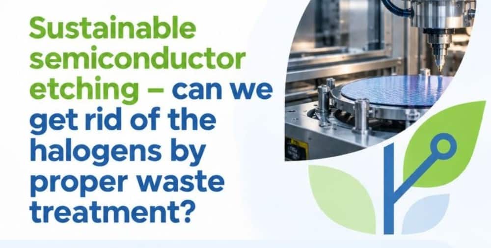
project HaloFreeEtch
Halogenated compounds are widely used in semiconductor fabrication, especially for etching small high aspect ratio structures. However, halogenated compounds such as SF6 come with an enormous carbon footprint and a high eco-toxicity. In the HaloFreeEtch project we will find out if there are alternative approaches for semiconductor etching without using halogenated etchants while keeping the process quality.
Agenda
13:00–13:15 – Welcome and Introduction to the topic | Dr. Jörg Schuster, TU Chemnitz
13:15–13:40 – LCA modeling of the BOSCH process – Impacts of the current abatement technologies and potential for further improvements | Saumya Sadhu, University of Graz
13:40–14:05 – Concepts and State of the Art for Abatement Systems | Stefanie Herrnberger, Pfeiffer Vacuum
14:05–14:40 – Abatement efficiencies and the impact of abatement on waste water | Pascal Osten and Sebastian Richard, DAS Environmental Experts
It is a webinar - the 3rd one organized within the EU-project Novel approaches for halogen-free and sustainable etching of Silicon and Glass.
Please register at the website: https://halofreeetch.eu/3rd-webinar/