Ansprechpartner
Day in the Fab: Life at Okmetic
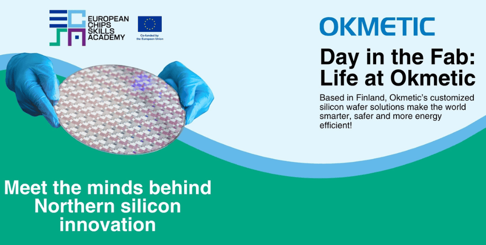
BILD: European Chips Skills Academy
Ever wondered what goes on inside a real semiconductor fab? Curious about how chips are made—or what it’s like to build your career in one?
On 15 September, the European Chips Skills Academy (ECSA) is teaming up with Okmetic to give you a virtual backstage pass to the world of chip innovation.
This interactive webinar is designed especially for students, recent graduates, and early-career professionals exploring futures in microelectronics and STEM fields. Whether you’re just getting started or looking to deepen your industry insights, this is your chance to see the semiconductor world up close—beyond textbooks and brochures.
Meet the People Behind the Chips
Hear from Eerika Kokkonen (SEMI Europe) and Jaska Tuominen (Okmetic) as they introduce how ECSA and Okmetic are working to connect talent with real-world opportunities in Europe’s growing chip industry.
Go Inside the Fab (Virtually!)
Take a tour through Okmetic’s cleanroom and discover how wafers are manufactured with precision, innovation, and teamwork.
Live Career Talks
Join Heikki Holmberg (R&D Director) and Nikita Bobrov (Process Engineer) for an honest conversation about what it’s like to work in a fab, build the future of semiconductors, and grow a career in this fast-evolving field.
Experts you will meet
Heikki Holmberg
Research and Development Director, Okmetic Oy
Heikki Holmberg is the Research and Development Director at Okmetic. With extensive semiconductor industry experience, Heikki has held multiple management roles, showcasing leadership and innovation. One of Heikki’s key areas of expertise is fostering efficient cooperation between universities and companies.
Nikita Bobrov
Process Development Engineer, Okmetic Oy
Nikita is a Process Development Engineer at Okmetic, specializing in semiconductor physics and microfabrication. His expertise has contributed to the development of multiple products and fabrication methods currently implemented in the company’s patterning and SOI production lines.
Why You Should Attend
Get real-world insights from professionals in the industry. Discover career pathways in chip manufacturing and process engineering and see where innovation happens— from R&D to the cleanroom. Learn how ECSA supports talent like you in navigating Europe’s chip ecosystem.
It’s free, it’s live, and it’s built for you. Don’t miss your chance to go inside the fab.
Further Links