Unternehmensart
Startseite | Mitglieder |
InnoLas Semiconductor GmbH
Mittlere Unternehmen (<250 Mitarbeiter:innen oder <50 Mio. Jahresumsatz)
Zielmärkte
Elektronik
Branchen
Produktion·Technologie
Portfolio
450mm·Beschriften·Equipment·Halbleiterindustrie·Laser·Lasermarking·Mikro- / Nanoelektronik·Sorter·sorting·Waferbeschriften·Wafersorter·wafersorting
Zertifikate
Kontakt
Neubruch 2
82266 Inning
82266 Inning
+49 (8143) 24195 -201
Ansprechpartner
Alexander Hofmann
+49 (8143) 24195 -201
Vertrieb / Sales
Über das Mitglied
High Quality Wafermarkier- & Wafersortiersysteme für die Halbleiterindustrie
Die InnoLas Semiconductor GmbH ist ein in Deutschland ansässiges, mittelständisches Unternehmen, das sich auf hochqualitative Wafermarkier- und Wafersortierlösungen für Kunden aus dem Halbleiterbereich spezialisiert. Seit über 25 Jahren ist es unser Kerngeschäft, individuelle auf den Kunden angepasste Lösungen zu entwickeln und zu fertigen.Bei allen im Portfolio befindlichen Maschinen legen wir allerhöchsten Wert auf die Auswahl von Subkomponenten, welche zu den qualitativ hochwertigsten auf dem Markt zählen. Die Montage und Inbetriebnahme erfolgt ausschließlich durch sehr erfahrene und gut ausgebildete Fachkräfte, sodass ein sehr hohes Maß an Qualität und Zuverlässigkeit erreicht wird. Um auch den höchsten Reinheitsanforderungen der Endkunden zu genügen, werden alle Anlagen im hauseigenen Reinraum ISO6 (ISO 14644-1) produziert und in Betrieb genommen.
Das Ziel ist es, unsere Kunden und Partner mit zuverlässigen und höchstqualitativen Systemen zu beliefern, welche zudem ein exzellentes Preis-Leistungsverhältnis besitzen. Die hohe Quote an langjährigen Stammkunden bestätigt unseren Qualitätsanspruch.
InnoLas Semiconductor GmbH ist ein Hersteller von Systemen für die Halbleiterindustrie. Unser Kerngeschäft liegt in der Markierung und/oder Sortierung von Halbleitersubtraten aller Größen und Materialien.
In der InnoLas Gruppe werden darüber hinaus folgende Systeme hergestellt:
- Laserstrahlquellen für Industrie und Wissenschaft
- Lasermaterialbearbeitung in der Solarindustrie
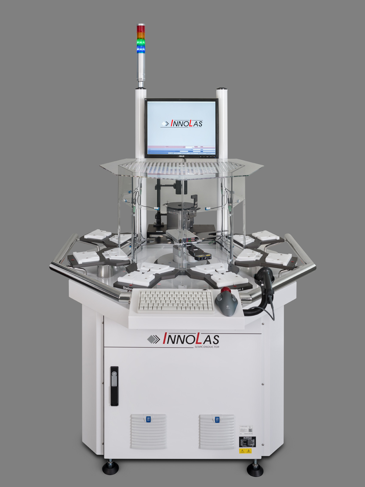
Laser Marking and Wafer Sorting System IL 2000 (2“ to 200 mm)
InnoLas Semiconductor develops and manufactures highly efficient processing systems for laser marking, sorting and the inspection of wafers for the semiconductor industry.
All marking and sorting processes meet the common industrial standards (SEMI, …) for the production of semiconductor wafers. State of the art laser quality, sophisticated automation, precise handling systems and advanced application software offer greater productivity and overall system reliability.
For wafer sizes from 2“ to 200 mm, InnoLas Semiconductor offers the IL 2000 series for wafer marking processes and the IL 2600 series as multi functional tools for wafer sorting, wafer merging/splitting and wafer inspection.
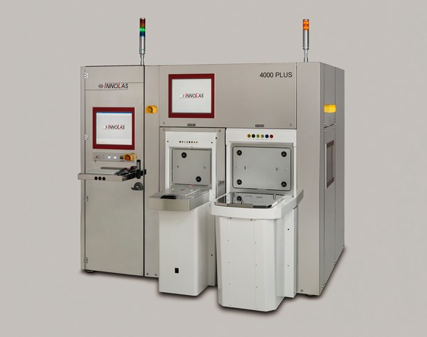
Laser Marking and Wafer Sorting System IL 4000 (300 / 450mm)
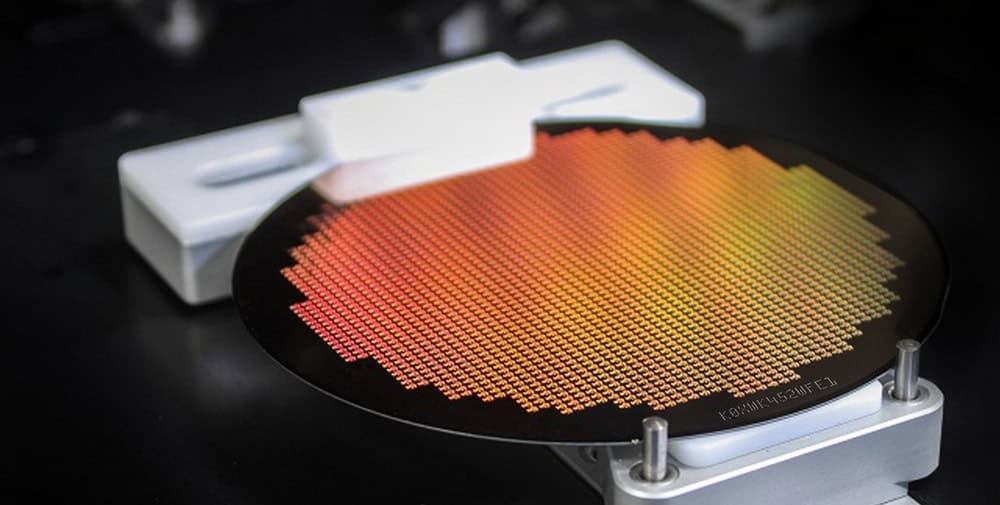
Wafers with a diameter of 450mm enable the Micro-chip industry an increase in yield of up to 80 percent. This leads to an enormous increase in productivity. In order to control the product quality these wafers receive a specific marking from the manufacturer.
Promptly at the start of the year, InnoLas Semiconductor GmbH, Technology leader in the market for sorting and laser marking systems for wafers, has successfully installed a second 450mm system. As an optional Bridge-Tool variant the system can mark 450mm and 300mm wafers on either side. The system checks the result automatically and thus reduces the process operations significantly. According to requirements, the customer can choose between vacuum handling and edge-grip handling. The latter transports the wafers especially carefully and cleanly.
The company places particular emphasis on in-house developments and products in the application of high-precision components. Together with the robust further development of proven engineering, this takes care of the constant high quality standard in marking and handling processes, also for the new wafer sizes.
“The marking and handling quality will be maintained at our high level for the new wafer sizes. To achieve this we use components developed in-house whenever the requirements are of high precision. These are otherwise not available in suitable quality as required by us and our customers,” said Andreas Behr, general manager of the InnoLas Semiconductor GmbH, explaining the consistently high standard achieved by his company’s wafer marking systems.
For more information, contact Alexander Hofmann at +49 (8143) 24195-201 or sales@il-semi.com or visit: www.innolas-semiconductor.com
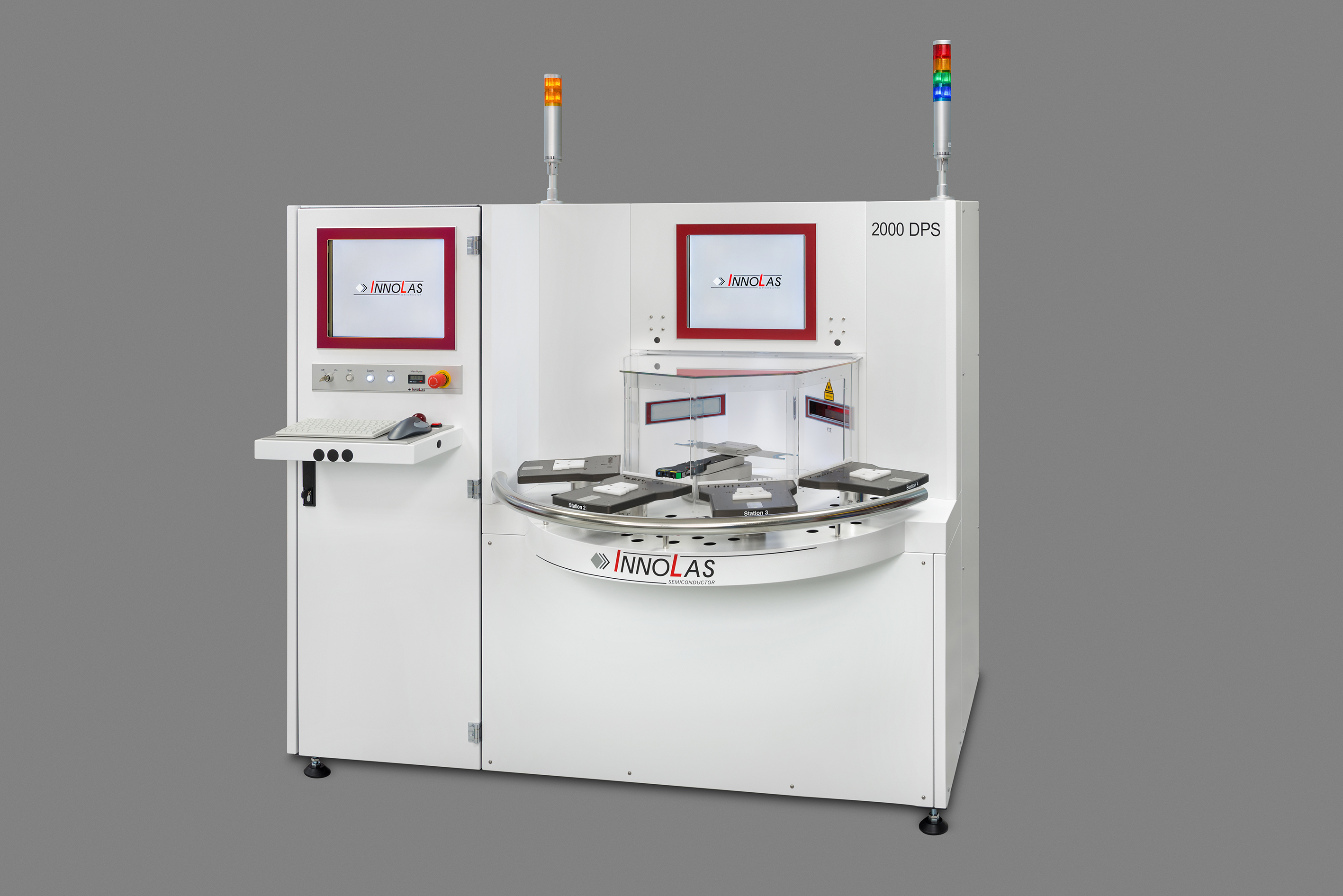
Wafer Sorting System IL 2600 (2" to 100mm / 100mm to 200mm)
The InnoLas IL 2600 wafer sorting system can automatically
sort, split, merge and transfer wafers from any slot / cassette to any other slot / cassette in a six cassette array. Wafer sizes from 2“ to 100mm and 100mm to 200mm can be handled in a single or multi-batch operation without the need of any mechanical adjustments. The laser mark code read for verification can be located at any position on the front and/or backside
of the wafer. The basic model has one reading unit (OCR, BC412,
T7) for reading the laser code on the frontside of the wafer. A second reading unit (OCR, BC412, T7) for reading the code on the backside of the wafer can be mounted as an option.
Standard Options
· Reading system for wafer front and / or backside
· Barcode hand scanner
· SECS/GEM host software
· Wafer thickness measurement